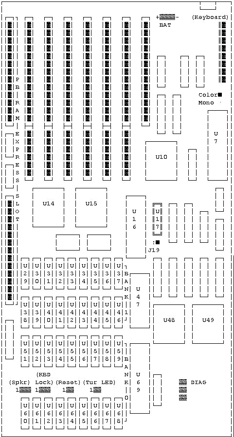
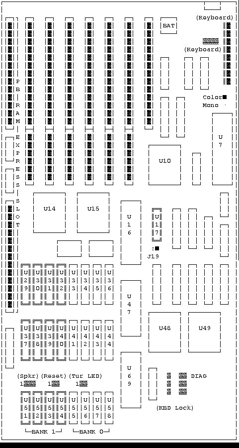
PB800/PB900 LAYOUT
NOTE:
There are two revisions of the PB800/900 motherboard.
1. LAYOUT
A. Revision C
NOTE:
Holds 1MB of RAM (256 x 1 chips), arranged in four rows
of nine chips per row (8 bits of ram and 1 parity bit.) The CMOS
backup battery is a removable AT style battery.
B. Revision D
NOTE:
Holds 1MB of RAM (256K x 4 chips) arranged in 2 rows of
4 and parity 1 row of 4 (256K x 1 chips) upgradeable to 2MB with
same chips plugged in adjacent sockets. CMOS Battery is soldered
2. SOCKETS
NOTE:
1. If chip at U14 is P82C212, BIOS must be 3.10.08a or 3.10.12
If chip at U14 is P82C212B, Bios must be 3.10.14
2. REV-D motherboard holds 2MB of RAM. Each Megabyte is (8) 256k
x 4 and (4) 256k x 1 chips for parity.
Socket |
Chip |
Description |
| U7 |
8042 |
Keyboard Controller |
| U10 |
83C206 |
|
| U14 |
82C212 or 82C212B |
|
| U15 |
80286 |
Main Processor |
| U16 |
80287 |
Math Coprocessor (optional) |
| U17 |
30-32MHZ |
Crystal (optional) |
| U47 |
|
BIOS (High) |
| U69 |
|
BIOS (Low) |
| U48 |
82C215 |
|
| U49 |
82C211C |
|
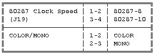
3. JUMPERS
NOTE
If a 80287-10 is installed you must also add a 30-32MHz
crystal at U17 in addition to setting the jumper.
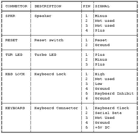
4. CONNECTORS
5. RISER CARD
NOTE: This system does not use a riser card.
Back to Main Menu