
See Also: Ram Upgrade Information Front Panel
| J | Description |
| J1 G3 | HD LED | ||
| J4 H1 | SIMM BANK 0 | ||
| J4 H2 | SIMM BANK 0 | ||
| J4 G1 | SIMM BANK 1 | ||
| J4 F1 | SIMM BANK 1 | ||
| J 7 J1 | IDE2 | ||
| J 8 J1 | FLOPPY | ||
| J 8 J2 | IDE | ||
| J 9 F1 | RISER SLOT | N/A | N/A |
| J 9 H1 | Auxilliary 3.3V Power | ||
| J 10 A1 | VESA | ||
| J 13 H5 | KEYBD | ||
| J 13 G1 | MOUSE | ||
| J 13 A1 | VIDEO | ||
| J 13 E1 | COM2 | ||
| J 13 F1 | COM1 | ||
| J 13 C1 | PARALLEL |
| J13A1 is a female DB15 VGA port built-in on the motherboard. |
J13C1: Parallel Port
| J13C1 is a female DB25 parallel port built-in on the motherboard. |
External Serial Port
| J13E1 and J13F1 is a male DB9 external serial port built-in on the motherboard. J13E1 is COM2. J13F1 is COM1. |
J13G1: PS/2 Mouse Port
| J13G1 is a female 6-pin mini DIN connector built-in on the motherboard. |
J13H5: PS/2 Keyboard Port
| J13H5 is a female 6-pin mini DIN connector built-in on the motherboard. |
J9F1: Riser Card Connector
| The riser card inserted in J9F1 can accommodate up to four 16-bit AT-compatible adapters and two 32-bit PCI adapters, or three 16-bit AT-compatible adapters and three 32-bit PCI adapters at any one time. |
U10J1: Battery
| U10J1 is a Dallas DS12887 real time clock and CMOS battery. |
J8J1: Floppy Drive Interface
| J9H1 is a male 2 x 17-pin floppy drive connector. |
J8J2: ISA Hard Drive Interface
| J9H2 is a male 2 x 20-pin ISA/IDE connector. |
J7J1: PCI Hard Drive Interface
| J9G1 is a male 2 x 20-pin PCI/IDE connector. |
J4F1 thru J4H1: SIMM Sockets
| Uses 1/2/4/8/16/32 MB 72-pin SIMMs, 70ns |
See Also: Ram Upgrade Information Front Panel
U10G1: Flash BIOS EEPROM
| This is the Flash BIOS EEPROM surface mounted on the motherboard. |
J9H1: PCI Bus Power Connector
| J9H1 is the 3.3V Power Connector for the PCI bus. |

J10A1: Video Feature Connector
Video Memory Upgrade Sockets
| Video memory can be upgraded to 2 MB by installing eight 256KBx4, 70ns VRAM ZIPs at locations U10C1, U10B5, U10B4, U10B3, U10B2, U10B1, U10A2, and U10A1. |
Also See: Video Upgrade Information Video Memory
| U8A1 and U8B4 make up the 1 MB video memory built-in on the motherboard. |
Also See: Video Upgrade Information Cache Memory
| U4A1 thru U6B2 make up the 256K L2 cache built-in on the motherboard. |
Also See: Cache Upgrade Information U4B2: CPU Socket
| At the moment, this socket can only accommodate the Pentium 60 processor. |
| Uses the 273-pin Type 4 CPU Socket. |
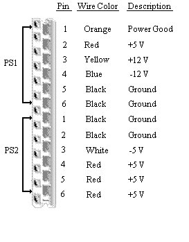
Also See: Cpu Upgrade Information Power Connector (PS1 / PS2)
J1G2: Turbo Switch 
J3A1: External Fan Connector 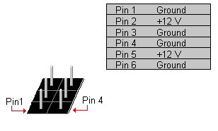
J7A1: CPU Clock 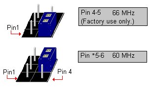
J12H1: Flash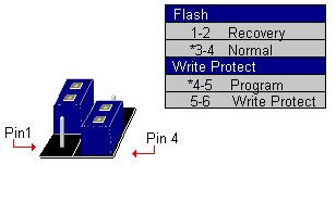
J13H1: CMOS and Password Options
J13H3: Monitor Setting 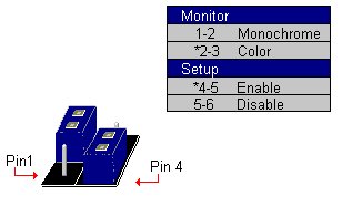
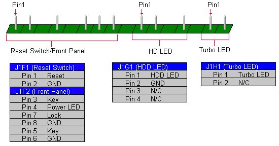
J1F1: Speaker