This information was extracted from a Windows .hlp file, XLX_TRM.HLP. Typographical errors have been left in this extracted version.
-mr_slug
Contents
System Specifications
Environmental and Regulatory Specifications
Connectors and Headers
Locations on the System Baseboard
Power and Ground Connector J0710
Power Connectors J0850 and J0860
Power Supply Enable Header J0861
Power and Ground Connector J0770
SIMM Sockets: J0550, J0551, J0650, and J0651
SCSI Disk Activity Header J0190
Onboard SCSI Headers J0060 and J0080
Parallel Connector J0600 (Top)
Video Connector J0600 (Bottom)
Keyboard and Mouse Connectors J0800
Peripherals
The Setup Program
EISA Configuration Utility
Running the EISA Configuration Utility
Video Drivers
Error and Informational Messages
Countdown Codes for Run-time Errors
System Baseboard Jumpers
Before You Begin Moving Jumpers
System Baseboard Jumper Options
Locations of Jumpers on the Baseboard
Floppy Protection Jumper E0291
Flash Reprogramming Power Jumper E0721
Baseboard Memory
Direct Memory Access (DMA) Channels
Spare Parts
Spare Parts (1-7) Illustration
Spare Parts (8-13) Illustration
Dimensions
Dimension | Specification |
Width | 21.54 cm (8.48 inches) |
Depth | 58.42 cm (23.0 inches) |
Height | 51.82 cm (20.4 inches) |
Weight | 20 kg (44.5 pounds) as shipped from the factory |
Environmental and Regulatory Specifications
Parameter | Specification |
Temperature |
|
Humidity |
|
Shock |
|
Vibration |
|
Altitude |
|
Maximum idle noise | Typical <42 dBA at 25�C with four internal hard disk drives (measured at 1 meter from the system with the peripherals idle). The noise of the variable-speed system fan will increase with temperature and power load. Note that the selection of peripherals may change the noise level. |
Electrostatic | Tested to 25 kV; no component damage |
AC Input Power |
|
Electromagnetic Interference (EMI) | FCC 47 Class B CFR Parts 2 and 15, Certified Class B |
Safety | UL 1950, 1st edition |
Power Supply
A 230 watt power supply that is switch-selectable for 115 (100 - 120) or 230 (200 - 240) VAC powers the X-series deskside/LX system. The table lists the output ratings for the power supply.
The table lists 150 watts available for +5 volts and 96 watts for +12�volts. You will have to adjust your loads so that the combined total wattage for your system configuration is less than 230 watts.
For information about calculating the power consumption for your system configuration, see your product guide.
The combined continuous current drainCurrentDrain.5 for -12 volts and -5 volts should not exceed 1 ampere. For example, if the current for -5 volts is 0.0 amperes, the maximum current rating for -12 volts goes to 1.0 ampere.
Voltage | Maximum Continuous | Minimum Load | Peak Surge | Watts |
+5 | 30.0 A | 3.0 A | 30.0 A | 150.0 W |
-5 | 0.5 A | 0.0 A | 0.5 A | 2.5 W |
+12 | 8.0 A | 0.25 A | 11.0 A | 96.0 W |
-12 | 1.0 A | 0.0 A | Maximum capacitive load <350 mF | 12.0 W |
Related Topics:
Current Drain
Current Drain
As an overall current drain limitation on the power supply, do not exceed the maximum output capacity of 30�amperes at +5 volts. The EISA slots on the system baseboard are rated at a maximum of 4.5�A per slot. The EISA specification recommends supporting an average of 2.0�A per slot. The average current consumption should not exceed 3.0�A per slot. The cooling efficiency varies per slot; therefore, ensure that adequate cooling is available in the target slot, especially in an expansion slot drawing more than 2.0 A.
Element | +5 V (typical) | +12 V | -12 V |
System baseboard (32�MB memory) | 4.0 A | 0.06 A | 0.06 A |
CPU Modules: |
|
|
|
Integrated cache CPU module (128 KB) | 2.5 A |
|
|
Cache modules: |
|
|
|
Memory module: |
|
|
|
3.5-inch floppy drive | 0.5 A |
|
|
EISA bus slot | 2.0 A |
|
|
Cooling fan |
| 0.3 A |
|
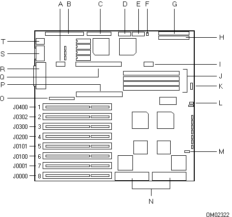
Locations on the System Baseboard
The top view of the system baseboard shows the location of the following connectors and headers:
A. J0710.8, CPU module power and ground connector
B. J0810.9, IDE header
C. J0840, 12-pin power connector
D. J0850, 6-pin power connector
E. J0860, 6-pin power connector
F. J0861, 2-pin power supply enable header
G. J0881, front panel header
H. J0880, floppy disk drive header
I. J0770, CPU module power and ground connector
J. J0650 and J0651, Bank 1 sockets; J0550 and J0551KGMPF9, Bank 0 sockets
K. J0590, speaker header
L. J0492, fan header
M. J0190, SCSI hard disk drive activity header
N. J0060, onboard SCSI header A; J0080N.LR_S, onboard SCSI header B
O. J0410, VESA-compatible 8514/A header
P. J0520, memory module connector
Q. J0730, CPU module main connector
R. J0600 (top), parallel connector and J0600 (bottom)PVG65R video connector
S. J0700, serial connectors (top: COM1, bottom: COM2)
T. J0800, PS/2-compatible keyboard (bottom) and PS/2-compatible mouse (top) connectors
Expansion slots:
J0400 EISA expansion slot 1, master
J0302 EISA expansion slot 2, master
J0300 EISA expansion slot 3, master
J0200 EISA expansion slot 4, master
J0101 EISA expansion slot 5, master
J0100 EISA expansion slot 6, master
J0001 EISA expansion slot 7, master
J0000 EISA expansion slot 8, master
The pin numbers for the headers and internal connectors are indicated on the system board.
Related Topics:
Top View of System Baseboard
Top View of System Baseboard
Power and Ground Connector J0710
Tag A in the baseboard illustration shows the location of the CPU module power and ground connector J0710, and the table below lists its pinout. (Tag Q shows the location of the CPU module main connector J0730. Tag I shows the location of the CPU module power and ground connector J0770.)
Pin # | Signal | Pin # | Signal |
1 | Ground | 2 | +5 V |
3 | Ground | 4 | +5 V |
5 | Ground | 6 | +5 V |
IDE Header J0810
Tag B in the baseboard illustration shows the location of the IDE header J0810, and the following table lists its pinout.
Pin # | Signal | Pin # | Signal |
1 | Reset | 2 | Ground |
3 | Data bit 7 | 4 | Data bit 8 |
5 | Data bit 6 | 6 | Data bit 9 |
7 | Data bit 5 | 8 | Data bit 10 |
9 | Data bit 4 | 10 | Data bit 11 |
11 | Data bit 3 | 12 | Data bit 12 |
13 | Data bit 2 | 14 | Data bit 13 |
15 | Data bit 1 | 16 | Data bit 14 |
17 | Data bit 0 | 18 | Data bit 15 |
19 | Ground | 20 | Key (pin missing) |
21 | DMA request 3 | 22 | Ground |
23 | I/O write | 24 | Ground |
25 | I/O read | 26 | Ground |
27 | I/O channel ready | 28 | Address latch enable |
29 | DMA acknowledge 3 | 30 | Ground |
31 | Interrupt request 14 | 32 | I/O channel size 16 |
33 | Address bit 1 | 34 | Ground |
35 | Address bit 0 | 36 | Address bit 2 |
37 | Host chip select 0 | 38 | Host chip select 1 |
39 | Disk activity | 40 | Ground |
Power Connector J0840
Tag C in the baseboard illustration shows the location of power connector J0840, and the following table lists its pinout. This 12-pin connector is keyed for two 6-pin power supply connectors PS1 and PS2. These 6-pin connectors are keyed and can be installed only in one way.
Pin # | Signal | P1 Color | Pin # | Signal | P2 Color |
1 | Power good | Orange | 7 | Ground | Black |
2 | +5 V | Red | 8 | Ground | Black |
3 | +12 V | Yellow | 9 | -5 V | White |
4 | -12 V | Blue | 10 | +5 V | Red |
5 | Ground | Black | 11 | +5 V | Red |
6 | Ground | Black | 12 | +5 V | Red |
Power Connectors J0850 and J0860
Tags D and E in the baseboard illustration show the location of the identical power connectors J0850 and J0860, and the following table lists their pinouts. One of the 6-pin P3 power supply connectors connects to J0850 and the other connects to J0860.
Pin # | Signal | P3 Color | Pin # | Signal | P3 Color |
1 | +5 V | Red | 4 | Ground | Black |
2 | +5 V | Red | 5 | Ground | Black |
3 | +5 V | Red | 6 | Ground | Black |
Power Supply Enable Header J0861
Tag F in the baseboard illustration shows the location of the power supply enable header J0861, and the following table lists its pinout.
Pin # | Signal | Color |
1 | Remote enable | Purple |
2 | Return | Black |
Front Panel Header J0881
Tag G in the baseboard illustration shows the location of the front panel header J0881, and the following table lists its pinout.
Pin # | Signal | Function |
1 | SPKDAT | Speaker data |
2 | +5 V | Speaker power |
3 | On/Off | Remote power enable |
4 | 0 V | Remote power return |
5 | FP Reset | Front panel reset |
6 | 0 V |
|
7 | Pwr LED | Power on LED |
8 | 0 V |
|
9 | SC 1 LED | SCSI controller 1 LED |
10 | SC 1 LED | SCSI controller 1 return |
11 | SC 2 LED | SCSI controller 2 LED |
12 | SC 2 LED | SCSI controller 2 return |
13 | KEYBD | Keyboard keylock |
14 | 0 V |
|
15 | +5 V |
|
16 | +5 V | LCD controller power/reset |
17 | (KEY) | (Missing pin) |
18 | +5V |
|
19 | RS | Register select |
20 | RW | Read/write |
21 | 0 V |
|
22 | EN | Enable |
23 | DB0 | I/O data 0 |
24 | DB1 | I/O data 1 |
25 | 0 V |
|
26 | DB2 | I/O data 2 |
27 | DB3 | I/O data 3 |
28 | DB4 | I/O data 4 |
29 | 0 V |
|
30 | DB5 | I/O data 5 |
31 | DB6 | I/O data 6 |
32 | DB7 | I/O data 7 |
33 | 0 V |
|
34 | 0 V |
|
Floppy Header J0880
Tag H in the baseboard illustration shows the location of floppy header J0880, and the following table lists its pinout.
Pin # | Signal | Pin # | Signal |
1 | Ground | 18 | Head direction |
2 | Density select | 19 | Ground |
3 | Ground | 20 | Step |
4 | Not connected | 21 | Ground |
5 | Key (pin missing) | 22 | Write data |
6 | Extended density in | 23 | Ground |
7 | Ground | 24 | Write enable |
8 | Index | 25 | Ground |
9 | Ground | 26 | Track 0 |
10 | Motor A on | 27 | Ground |
11 | Ground | 28 | Write protect |
12 | Drive B select | 29 | Extended density out |
13 | Ground | 30 | Read data |
14 | Drive A select | 31 | Ground |
15 | Ground | 32 | Head select side 1 |
16 | Motor B on | 33 | High density out |
17 | Ground | 34 | Disk change |
Power and Ground Connector J0770
Tag I in the baseboard illustration shows the location of the CPU module power and ground connector J0770, and the following table lists its pinout. (Tag Q shows the location of the CPU module main connector J0730. Tag A shows the location of the CPU module power and ground connector J0710.)
Pin # | Signal | Pin # | Signal |
1 | Ground | 2 | Vcc |
3 | Reserved | 4 | Reserved |
5 | Reserved | 6 | Vcc |
SIMM Sockets: J0550, J0551, J0650, and J0651
Tag J in the baseboard illustration shows the location of SIMM sockets J0550, J0551, J0650, and J0651 for memory banks 0 and 1. The following table lists the memory banks and their associated SIMM sockets.
Bank | Socket |
0 | J0550 |
0 | J0551 |
1 | J0650 |
1 | J0651 |
Speaker Header J0590
Tag K in the baseboard illustration shows the location of speaker header J0590, and the following table lists its pinout.
Pin # | Signal |
1 | SPKDAT (speaker data) |
2 | No connection |
3 | No connection |
4 | Return |
Fan Header J0492
Tag L in the baseboard illustration shows the location of fan header J0492, and the following table lists its pinout.
Pin # | Signal |
1 | Ground |
2 | +12 V |
3 | Ground |
SCSI Disk Activity Header J0190
Tag M in the baseboard illustration shows the location of the SCSI disk activity header J0190, and the following table lists its pinout.
Front Panel LED #1 | Front Panel LED #2 | ||
Pin # | Signal | Pin # | Signal |
1 | Not connected | 3 | Hard disk active |
2 | Hard disk active | 4 | Not connected |
Onboard SCSI Headers J0060 and J0080
Tag N in the baseboard illustration shows the location of the channel A and B headers for the onboard Adaptec AIC-7770 dual SCSI controller. The following table lists the pinouts for headers A, J0060, and B, J0080; they are identical.
Pin # | Signal | Pin # | Signal |
1 | Ground | 26 | -DB0 |
2 | Ground | 27 | -DB1 |
3 | Ground | 28 | -DB2 |
4 | Ground | 29 | -DB3 |
5 | Ground | 30 | -DB4 |
6 | Ground | 31 | -DB5 |
7 | Ground | 32 | -DB6 |
8 | Ground | 33 | -DB7 |
9 | Ground | 34 | -DBP |
10 | Ground | 35 | Ground |
11 | Ground | 36 | Ground |
12 | Reserved | 37 | Reserved |
13 | Open | 38 | Termpwr |
14 | Reserved | 39 | Reserved |
15 | Ground | 40 | Ground |
16 | Ground | 41 | -ATN |
17 | Ground | 42 | Ground |
18 | Ground | 43 | -BSY |
19 | Ground | 44 | -ACK |
20 | Ground | 45 | -RST |
21 | Ground | 46 | -MSG |
22 | Ground | 47 | -SEL |
23 | Ground | 48 | -C/D |
24 | Ground | 49 | -REQ |
25 | Ground | 50 | -I/O |
* The minus sign next to the signal indicates active low.
8514/A Header J0410
Tag O in the baseboard illustration shows the location of the 8514/A header J0410, and the following table lists its pinout.
Pin # | Signal | Pin # | Signal |
1 | Ground | 2 | Pixel data 0 |
3 | Ground | 4 | Pixel data 1 |
5 | Ground | 6 | Pixel data 2 |
7 | Enable external pixel data | 8 | Pixel data 3 |
9 | Enable external sync | 10 | Pixel data 4 |
11 | Enable external pixel clock | 12 | Pixel data 5 |
13 | Not connected | 14 | Pixel data 6 |
15 | Ground | 16 | Pixel data 7 |
17 | Ground | 18 | Pixel clock |
19 | Ground | 20 | Blanking |
21 | Ground | 22 | Horizontal sync |
23 | Not connected | 24 | Vertical sync |
25 | Key (pin missing) | 26 | Ground |
Memory Module Connector J0520
Tag P in the baseboard illustration shows the location of the memory module connector J0520, and the following table lists its pinout.
Pin # | Signal | Pin # | Signal |
1 | Hard reset | 2 | Ground |
3 | Reserved | 4 | Reserved |
5 | Reserved | 6 | 64 bit operation |
7 | +5 V | 8 | Reserved |
9 | Correctable ECC error | 10 | Disable ECC |
11 | Error | 12 | Force parity error on writes |
13 | Partition select 1 | 14 | Ground |
15 | Partition select 3 | 16 | Remap |
17 | Remapping address 17 | 18 | Memory bus access |
19 | +5 V | 20 | Partition select 0 |
21 | Remapping address 18 | 22 | Partition select 2 |
23 | Remapping address 19 | 24 | Write protect |
25 | Memory speed 0 | 26 | Ground |
27 | Memory speed 1 | 28 | Memory cache enable |
29 | Lock | 30 | Response 0 |
31 | +5 V | 32 | Response 1 |
33 | Status 0 | 34 | Ready |
35 | Status 1 | 36 | Reserved |
37 | Status 2 | 38 | Ground |
39 | Ground | 40 | Address strobe |
41 | CAS latch even | 42 | Ground |
43 | CAS latch odd | 44 | Odd memory bank select |
45 | Ground | 46 | Even memory bank select |
47 | Byte enable 1 | 48 | Ground |
49 | Byte enable 3 | 50 | Byte enable 0 |
51 | Address bit 3 | 52 | Byte enable 2 |
53 | Address bit 5 | 54 | +5 V |
55 | +5 V | 56 | Address bit 2 |
57 | Address bit 7 | 58 | Address bit 4 |
59 | Address bit 9 | 60 | Address bit 6 |
61 | Address bit 11 | 62 | Ground |
63 | Address bit 13 | 64 | Address bit 8 |
65 | +5 V | 66 | Address bit 10 |
67 | Address bit 15 | 68 | +5 V |
69 | Address bit 17 | 70 | Address bit 12 |
71 | Ground | 72 | Address bit 14 |
73 | Address bit 19 | 74 | Address bit 16 |
75 | Address bit 21 | 76 | Address bit 18 |
77 | Address bit 23 | 78 | +5 V |
79 | +5 V | 80 | Address bit 20 |
81 | Address bit 25 | 82 | Address bit 22 |
83 | Address bit 27 | 84 | Address bit 24 |
85 | Ground | 86 | Address bit 26 |
87 | Address bit 29 | 88 | Ground |
89 | Address bit 31 | 90 | Address bit 28 |
91 | Ground | 92 | Address bit 30 |
93 | Data bit 1 | 94 | Ground |
95 | Ground | 96 | Data bit 0 |
97 | Data bit 3 | 98 | Data bit 2 |
99 | Data bit 5 | 100 | Data bit 4 |
101 | Data bit 7 | 102 | +5 V |
103 | Data bit 9 | 104 | Data bit 6 |
105 | Data bit 11 | 106 | Data bit 8 |
107 | Ground | 108 | Data bit 10 |
109 | Data bit 13 | 110 | Data bit 12 |
111 | Data bit 15 | 112 | Data bit 14 |
113 | Data bit 17 | 114 | +5 V |
115 | Data bit 19 | 116 | Data bit 16 |
117 | Data bit 21 | 118 | Data bit 18 |
119 | Ground | 120 | Data bit 20 |
121 | Data bit 23 | 122 | Data bit 22 |
123 | Data bit 25 | 124 | Data bit 24 |
125 | Data bit 27 | 126 | +5 V |
127 | Data bit 29 | 128 | Data bit 26 |
129 | Data bit 31 | 130 | Data bit 28 |
131 | Ground | 132 | Data bit 30 |
CPU Module Connector J0730
Tag Q in the baseboard illustration shows the location of the CPU module main connector J0730, and the following table lists its pinout. (Tag A in the baseboard illustration shows the location of the CPU module power and ground connector J0710. Tag I shows the location of the CPU module power and ground connector J0770.)
Pin # | Signal | Pin # | Signal |
1 | Hard reset | 2 | Ground |
3 | Bus grant | 4 | Soft reset |
5 | Bus request | 6 | 64 bit operation |
7 | +5 V | 8 | Refresh request |
9 | Allow 20 mask | 10 | Refresh demand |
11 | Memory bus access | 12 | Reset numeric processor exception error |
13 | Cache flush | 14 | Ground |
15 | Write modified cache entries | 16 | Interrupt request 13 |
17 | Maskable interrupt | 18 | Nonmaskable interrupt |
19 | +5 V | 20 | Cache data modified |
21 | Snoop status available | 22 | Snoop strobe |
23 | Write through / write back | 24 | Write protect |
25 | Memory speed 0 | 26 | Ground |
27 | Memory speed 1 | 28 | Memory area cacheable |
29 | Lock | 30 | Response 0 |
31 | +5 V | 32 | Response 1 |
33 | Status 0 | 34 | Ready |
35 | Status 1 | 36 | Force access termination |
37 | Status 2 | 38 | Ground |
39 | Ground | 40 | Address strobe |
41 | CAS latch even | 42 | Ground |
43 | CAS latch odd | 44 | Odd memory bank select |
45 | Ground | 46 | Even memory bank select |
47 | Byte enable 1 | 48 | Ground |
49 | Byte enable 3 | 50 | Byte enable 0 |
51 | Address bit 3 | 52 | Byte enable 2 |
53 | Address bit 5 | 54 | +5 V |
55 | +5 V | 56 | Address bit 2 |
57 | Address bit 7 | 58 | Address bit 4 |
59 | Address bit 9 | 60 | Address bit 6 |
61 | Address bit 11 | 62 | Ground |
63 | Address bit 13 | 64 | Address bit 8 |
65 | +5 V | 66 | Address bit 10 |
67 | Address bit 15 | 68 | +5 V |
69 | Address bit 17 | 70 | Address bit 12 |
71 | Ground | 72 | Address bit 14 |
73 | Address bit 19 | 74 | Address bit 16 |
75 | Address bit 21 | 76 | Address bit 18 |
77 | Address bit 23 | 78 | +5 V |
79 | +5 V | 80 | Address bit 20 |
81 | Address bit 25 | 82 | Address bit 22 |
83 | Address bit 27 | 84 | Address bit 24 |
85 | Ground | 86 | Address bit 26 |
87 | Address bit 29 | 88 | Ground |
89 | Address bit 31 | 90 | Address bit 28 |
91 | Ground | 92 | Address bit 30 |
93 | Data bit 1 | 94 | Ground |
95 | Ground | 96 | Data bit 0 |
97 | Data bit 3 | 98 | Data bit 2 |
99 | Data bit 5 | 100 | Data bit 4 |
101 | Data bit 7 | 102 | +5 V |
103 | Data bit 9 | 104 | Data bit 6 |
105 | Data bit 11 | 106 | Data bit 8 |
107 | Ground | 108 | Data bit 10 |
109 | Data bit 13 | 110 | Data bit 12 |
111 | Data bit 15 | 112 | Data bit 14 |
113 | Data bit 17 | 114 | +5 V |
115 | Data bit 19 | 116 | Data bit 16 |
117 | Data bit 21 | 118 | Data bit 18 |
119 | Ground | 120 | Data bit 20 |
121 | Data bit 23 | 122 | Data bit 22 |
123 | Data bit 25 | 124 | Data bit 24 |
125 | Data bit 27 | 126 | +5 V |
127 | Data bit 29 | 128 | Data bit 26 |
129 | Data bit 31 | 130 | Data bit 28 |
131 | Ground | 132 | Data bit 30 |
Parallel Connector J0600 (Top)
Tag R in the baseboard illustration shows the location of the two-tiered connector J0600. The top tier is the parallel connector, and the bottom tier is the video connector. The following table lists the pinout for the parallel connector, and the illustration shows the connector.
Pin # | Signal | Pin # | Signal |
1 | Strobe | 10 | Acknowledge |
2 | Data bit 0 | 11 | Busy |
3 | Data bit 1 | 12 | Paper end |
4 | Data bit 2 | 13 | Select |
5 | Data bit 3 | 14 | Auto feed |
6 | Data bit 4 | 15 | Error |
7 | Data bit 5 | 16 | Initialize printer |
8 | Data bit 6 | 17 | Select input |
9 | Data bit 7 | 18 - 25 | Ground |
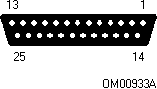
Video Connector J0600 (Bottom)
Tag R in the baseboard illustration shows the location of the two-tiered connector J0600. The bottom tier is the video connector, and the top tier is the parallel connector. The following table lists the pinout for the video connector, and the illustration shows the connector.
Pin # | Signal | Pin # | Signal |
1 | Red | 10 | Ground |
2 | Green | 11 - 12 | Not connected |
3 | Blue | 13 | Horizontal sync |
4 | Not connected | 14 | Vertical sync |
5 - 8 | Ground | 15 | Not connected |
9 | Not connected |
|
|

Serial Connectors J0700
Tag S in the baseboard illustration shows the location of the two-tiered serial connector J0700. The top tier is COM1, and the bottom tier is COM2. The following table lists the pinout for these identical connectors. The illustration shows a serial connector.
Pin # | Signal | Pin # | Signal |
1 | Data carrier detect | 6 | Data set ready |
2 | Receive data | 7 | Request to send |
3 | Transmit data | 8 | Clear to send |
4 | Data terminal ready | 9 | Ring indicator |
5 | Ground |
|
|

Keyboard and Mouse Connectors J0800
Tag T in the baseboard illustration shows the location of the two-tiered connector J0800. The top tier is the mouse connector, and the bottom tier is the keyboard connector. The following table lists their identical pinouts. The illustration shows a connector.
Pin # | Signal | Pin # | Signal |
1 | Data | 4 | +5 V (fused) |
2 | Not connected | 5 | Clock |
3 | Ground | 6 | Not connected |

3.5-inch, Diskette Drive
The table lists the electrical requirements for the 1.44 MB, 3.5-inch diskette drive.
Attribute | Specification |
Voltage range | +5 V (-6%, +10%) |
Ripple | 100 mV peak-to-peak max |
Operating mode |
|
Stand-by | 7.0 mA typical, 9.0 mA max |
Read | 0.28 A typical, 0.40 A max |
Write | 0.34 A typical, 0.46 A max |
3 ms seek | 0.52 A typical, 0.66 A max |
6 ms seek | 0.66 A typical, 0.80 A max |
Motor start | 0.66 A typical, 0.80 A max |
Introduction
You can configure your X-series deskside/LX system by using one of the following methods:
� the system BIOS Setup Utility, which is stored in both the flash memory and the batterybacked memory of the real-time clock (RTC)
� the EISA Configuration Utility (ECU) on the System Configuration Disk which was shipped with the system
If your system does not have a diskette drive or it is disabled, use Setup to configure your system. Otherwise, use the ECU to configure it. The information you enter using the ECU overrides any entered using Setup.
If your diskette drive is disabled or improperly configured, you must use Setup to enable it so that you can use the ECU. If necessary, you can disable the drive after you exit the ECU.
Turning on Your System
Use the following procedure to turn on your system:
1. Make sure all external devices, such as a video display monitor, keyboard, and mouse, have been connected.
2. Remove drive protection cards (if present) from the diskette drive(s) and tape drive (if installed).
3. Before you connect the AC power cord to the system, make sure that the line voltage selector switch on the back panel is set to the correct line source voltage (see your product guide).
4. Make sure that the power cord is connected to the AC power input socket on the back of the system.
5. Make sure that the male connector of the power cord is plugged into a grounded AC electrical outlet. Refer to your product guide.
6. Turn on the video display monitor.
7. Turn on your system by pressing the power on/off push-button switch on the front panel (see your product guide).
8. Verify that the power indicator light on the front panel is lit (see your product guide).
9. After a few seconds your system begins a power-on self test. (POST).
Power-on Self-Test
Each time you turn on the X-series system, the power-on self-test (POST) runs automatically and checks the system baseboard, CPU module, memory, keyboard, and most installed peripheral devices.
During the memory test, POST displays the amount of memory that it was able to access and test. Depending on the amount of memory installed, it may take several minutes to complete the memory test. If you do not want to wait for the memory test to complete, you can terminate it after it starts by pressing [Spacebar]. After a soft boot ([Ctrl] + [Alt] + [Del]), POST does not test the memory. Depending on your system configuration, you may or may not see the following message on your video display monitor:
Press Spacebar to Abort Memory Test
Whether or not the above message appears on your video display monitor, the [Spacebar] remains active.
When POST reaches countdown number 135, the system beeps twice and, depending on your system configuration, may or may not display a message similar to the following:
To continue press:...................Spacebar
To configure system press:.................F1
If you do not press the spacebar or [F1], the above message remains for a few seconds, the system beeps once, and then the boot process continues. The [Spacebar] and [F1] remain active whether or not the above message appears on your monitor.
If the system halts before POST completes running, it will emit a beep code indicating a fatal system error that requires immediate attention. For a listing of beep codes and error messages that POST can generate, refer to "Error and Informational Messages."
Running Setup
The Setup utility, located in flash memory on the system baseboard, enables you to check or change the baseboard configuration information. It does not allow you to enter or change information about EISA add-in boards. Setup stores most of the configuration values in the battery-backed memory of the real-time clock (RTC); the rest of the values are stored in the flash EPROM. The values take effect when you boot up the system. POST. checks the values against the actual hardware configuration; if they do not agree, it generates an error message. You must then run Setup to specify the correct configuration.
You can run the Setup utility with or without an operating system being present.
Setup displays four pages of configuration fields: Setup Page 1, Setup Page 2, Setup Page 3, and Setup Page 4. To move from one Setup page to another, press [Pg Up] or [Pg Dn]. To select a field, use [Up] or [Down] to move the cursor to the field; the cursor moves only to the fields that you can change. Use [+] or [-] to change the value of the selected field. Each time you press [+] or [-], Setup displays one of the possible values of the field.
To save the configuration information and reboot the system so that the changes take effect, press [Esc] and then [F4].
Since values entered using the Setup utility are overwritten when you run the EISA Configuration Utility (ECU), you should only run Setup under the following conditions:
� To enable your diskette drive
� If you do not have access to a diskette drive
� If you have installed only ISA expansion boards in your system
Setup Page 1
This section describes the configuration fields displayed on Setup page�1. The default value for each field is in boldface type. Press [Pg Up] or [Pg Dn] until the page appears.
Related Topics:
System Time
System Date
Onboard Floppy
Diskette A
Diskette B
Onboard IDE
Hard Drive 1
Hard Drive 2
Onboard SCSI
SCSI BIOS Mapping
User Definable Drives
System Time
The System Time field contains three option fields: hours, minutes, and seconds. Use [up] or [down] to highlight the field that you want to change, and then press [+] or [-] to change it (the seconds field only resets to 0). If you hold down [+] or [-], the value changes continuously. The new time takes effect immediately; you don't have to reboot the system.
System Date
The System Date field contains three option fields: day of the month, month, and year. Use [up] or [down] to highlight the field that you want to change, and then press [+] or [-] to change it. The new date takes effect immediately; you don't have to reboot the system.
Onboard Floppy
The Onboard Floppy field lets you enable or disable the onboard diskette drive controller. Select Enabled if you are using the onboard controller to control the diskette drive. If you select Disabled, then interrupt (IRQ 6) is available for an addin board to use. Use [up] or [down] to highlight the field, and then press [+] or [-] to change it. The options include:
� Enabled
� Disabled
For additional security, you can disable writing to the diskette drive with the floppy protection jumper. Refer to "Floppy Protection Jumper E0291"
Diskette A
Use [up] or [down] to highlight the Diskette A field, and then press [+] or [-] to change to the appropriate diskette type. The options include:
� 5.25", 360 KB
� 5.25", 1.2 MB
� 3.5", 720 KB
� 3.5", 1.44 MB
� 3.5", 2.88 MB
� Not Installed
Note: The media detection code signals may be grounded by some diskette drive types. If so, you may need to install a different signal cable from the system baseboard to the diskette drive.
Diskette B
Use [up] or [down] to highlight the Diskette B field, and then press [+] or [-] to change to the appropriate diskette type. The options include:
� 5.25", 360 KB
� 5.25", 1.2 MB
� 3.5", 720 KB
� 3.5", 1.44 MB
� 3.5", 2.88 MB
� Not Installed
Onboard IDE
The Onboard IDE field lets you enable or disable the onboard IDE controller. Enable the field if you are using an IDE hard disk drive in an internal drive bay. If you disable the field, then the IDE disk hardware interrupt (IRQ�14) is available for an addin board to use. Use [up] or [down] to highlight the field, and then press [+] or [-] to change it. The options include:
� Enabled
� Disabled
Hard Drive 1
The Hard Drive 1 field lets you specify the drive type for hard disk drive C.
CAUTION: You must specify the correct hard disk drive type, because the system BIOS cannot independently verify this information. The system BIOS will not recognize the installed hard disk drive if the drive type is incorrect.
Note: We do not recommend mounting a hard disk drive in a 5.25-inch external peripheral bay because the drive may generate EMI. In addition, its susceptibility to ESD increases in the external bay.
Contact your sales representative or dealer for a list of approved add-in peripheral devices.
Select "Not Installed" if a SCSI hard disk drive is installed or if no hard disk drive is installed. If only one drive is installed, it will always be Hard Drive 1. In this case, select "Not Installed" for Hard Drive.
For information about the drive type, refer to the manufacturer's documentation packaged with the drive. Some manufacturers provide the drive parameters rather than the drive type.
If you know the drive type, use [up] or [down] to highlight the Hard Drive 1 field, and then press [+] or [-] until your drive type appears on the screen. For each drive type, the drive parameters also appear on the screen. The options include:
� Not Installed
� Type 1
through
� Type 47
If you have only the drive parameters, try to match them by stepping through the drive types and checking the displayed parameters for each type. If there is no match, select one of the user-definable drive types (2 and 3 or 48 and 49) to specify your drive's parameters. See "User Definable Drives."
Hard Drive 2
The Hard Drive 2 field lets you specify the drive type for hard disk drive D. The options are the same as those listed for hard drive.
Onboard SCSI
Depending on the model, the X-series deskside/LX system baseboard contains an onboard Adaptec AIC-7770, 32-bit dual channel SCSI controller. Enable H/W Only if the system does not boot up from a SCSI device connected to the embedded onboard SCSI controller, such as when you have only SCSI tape drives or CDROM drives installed; in this case, the SCSI drivers must be installed after running Setup. Enable H/W�&�BIOS if the system boots up from a SCSI device. Disable the Onboard SCSI field if you do not have SCSI devices connected to the system. Use [up] or [down] to highlight the field, and then press [+] or [-] to change it. The options include:
� Disabled
� H/W Only
� H/W & BIOS
SCSI, when enabled, uses hardware interrupt 11 by default. When SCSI is disabled, interrupt 11 is available. Use the ECU to edit the interrupts.
The Onboard SCSI field refers only to the SCSI controller, not the installed SCSI devices. To fully enable the Onboard SCSI field, you must run the ECU. See "Running the EISA Configuration Utility."
Note: If the onboard SCSI BIOS is enabled, it must not conflict with another system BIOS; for example, if the video BIOS is at E0000H, then the SCSI BIOS must be at a different address.
Run EZ-SCSI to install SCSI devices in your system when you are using DOS as your operating system. For information about running EZ-SCSI, see your X-Series SCSI Software User's Guide for the AIC-7770.
SCSI BIOS Mapping
If the onboard SCSI BIOS is enabled, it must not conflict with the onboard video BIOS; for example, if the onboard video BIOS3B8A0M4 is at E0000H, then the SCSI BIOS must be at a different address. Enabling the onboard SCSI BIOS in Setup assigns it to interrupt 11. Use [up] or [down] to highlight the field, and then press [+] or [-] to change it. The options include:
� C0000H
� C8000H
� E0000H
� EC000H
User Definable Drives
The User Definable Drives field allows you to enable the user-definable drive types 2 and 3 or 48 and 49. Select 48 and 49 unless there is a conflict with your network; if there is, select 2 and 3. Use [up] or [down] to highlight the field, and then press [+] or [-] to change it. The options include:
� 2 and 3
� 48 and 49
After you select one of the user-definable drive types, press [up] to highlight the drive parameter fields. Enter the parameters supplied by the manufacturer.
Setup Page 2
This section describes the configuration fields displayed on Setup page 2. The default value for each field is in boldface type. Press [Pg Up] or [Pg Dn] until the page appears.
Related Topics:
Video Type
640 x 480 Mode Refresh Rate
800 x 600 Mode Refresh Rate
1024 x 768 Mode Refresh Rate
Video Font
Onboard Video Controller1
Offboard VGA/EGA Adapter Installed
Keyboard
NumLock on at Boot
Password
POST Memory Test Prompt
POST Setup Prompt
Boot Device Select
Video Type
The Video Type field lets you specify the onboard video display type. If you have installed an add-in video controller board, select the option that describes it. Use [up] or [down] to highlight the field, and then press [+] or [-] to change it. The options include:
� VGA/EGA
� CGA40
� CGA80
� MDA
� Not Installed
When you select the Not Installed option, the display type will be configured for VGA.
480 Mode Refresh Rate
The 640 x 480 Mode Refresh Rate field lets you select the appropriate refresh rate for your video display monitor. A higher refresh rate means less vertical flicker, and therefore less eyestrain. The refresh rate you choose depends on the monitor type you select when you configure your system. This feature is valid only when the onboard video is used. Use [up] or [down] to highlight the field, and then press [+] or [-] to change it. The options include:
� 60 Hz
� 75 Hz
� x2, x16 @ 72 Hz
CAUTION: It is possible to damage your monitor if you use the incorrect refresh rate. Check the documentation that came with your monitor to determine the proper setting.
800 x 600 Mode Refresh Rate
The 800 x 600 Mode Refresh Rate field lets you select the appropriate refresh rate for your video display monitor. A higher refresh rate means less vertical flicker, and therefore less eyestrain. The refresh rate you choose depends on the monitor type you select when you configure your system. This feature is valid only when the onboard video is used. Use [up] or [down] to highlight the field, and then press [+] or [-] to change it. The options include:
� 56 Hz
� 60 Hz
� 72 Hz
CAUTION: It is possible to damage your monitor if you use the incorrect refresh rate. Check the documentation that came with your monitor to determine the proper setting.
1024 x 768 Mode Refresh Rate
The 1024 x 768 Mode Refresh Rate field lets you select the appropriate refresh rate for your video display monitor. A higher refresh rate means less vertical flicker, and therefore less eyestrain. The refresh rate you choose depends on the monitor type you select when you configure your system. This feature is valid only when the onboard video is used. Use [up] or [down] to highlight the field, and then press [+] or [-] to change it. The options include:
� Interlaced @ 44/88 Hz
� Non-Interlaced @ 60 Hz
� Non-Interlaced @ 70 Hz
� Non-Interlaced @ 72 Hz
CAUTION: It is possible to damage your monitor if you use the incorrect refresh rate. Check the documentation that came with your monitor to determine the proper setting.
Video Font
The Video Font field lets you select video character font dimensions. The 9�x�16 font is recommended for general use with VGA and most application and utility programs. Use [up] or [down] to highlight the field, and then press [+] or [-] to change it. The options include:
� 9 x 16
� 8 x 16
Onboard Video Controller
In a two-monitor system, the Onboard Video Controller field lets you select the appropriate option according to whether the video display monitor connected to the onboard video controller is the primary or the secondary monitor. All BIOS video writes are directed to the primary video display monitor. This feature is valid only when the onboard video is used. Use [up] or [down] to highlight the field, and then press [+] or [-] to change it. The options include:
� Primary
� Secondary
The super VGA controller on the system baseboard is a Western Digital WD90C31.
Offboard VGA/EGA Adapter Installed
The Offboard VGA/EGA Adapter Installed field allows you to indicate whether there is an offboard video BIOS at C0000H or not. If you install a VGA/EGA adapter board in your system, select "Yes" so that the offboard video BIOS will be initialized during the video initialization phase early in POST. Use [up] or [down] to highlight the field, and then press [+] or [-] to change it. The options include:
� No
� Yes
The options for the Offboard VGA/EGA Adapter Installed field do not affect the onboard video controller. To disable it, refer to procedure "VGA Jumper E0290."
Keyboard
The Keyboard field lets you enable or disable error reporting for the keyboard. If you are going to operate your system without a keyboard, select "Not Installed" so that POST will not report the absence of the keyboard as an error: for example, as a network server. If you use a keyboard with the field set to "Not Installed," it will function normally as when running Setup. Use [up] or [down] to highlight the field, and then press [+] or [-] to change it. The options include:
� Not Installed
� Installed
Regardless of whether or not you select either "Installed" or "Not Installed," the system does not wait indefinitely for input from the keyboard.
NumLock on at Boot
The NumLock field lets you enable or disable the "Num Lock" key after the system boots up. If you change the value of the field, your system will boot up the next time with the value you chose. Use [up] or [down] to highlight the field, and then press [+] or [-] to change it. The options include:
� No
� Yes
Password
The Password field permits you to install a password. If you install one, it must be entered when you power up the system or the system will not boot. Use [up] or [down] to highlight the field.
� Not installed
To install a password, press [+] or [-] and follow the instructions displayed on the screen. After you install a password, the Password field switches to "Installed." The next time you reboot the system, it will prompt you for the password.
To change the password, boot up the system and enter the following at the prompt:
Enter Password: oldpassword/newpassword/newpassword
To remove the password, boot up the system and enter the following at the prompt:
Enter Password: password/
To disable the password facility, set the password jumper to "Off" on the system baseboard. Refer to "Password Jumper E0390."
POST Memory Test Prompt
The POST Memory Test Prompt field lets you enable or disable the memory test prompt. Use [up] or [down] to highlight the field, and then press [+] or [-] to change it. The options include:
� Enabled
� Disabled
When the field is enabled, the following message appears on the video display monitor during the memory test:
Press Spacebar to Abort Memory Test
POST Setup Prompt
The POST Setup Prompt field lets you enable or disable the setup prompt. Use [up] or [down] to highlight the field, and then press [+] or [-] to change it. The options include:
� Enabled
� Disabled
If the field is enabled, the following message appears on the video display monitor when POST reaches countdown number 135:
To continue press:...................Spacebar
To configure system press:.................F1
If the field is disabled, the above message will not appear on the video display monitor. However, when POST reaches countdown number 135, it pauses for a few seconds so that you can press either the [Spacebar] or [F1].
Whether or not the above message appears on your video display monitor, the [Spacebar] and [F1] remain active.
Boot Device Select
The Boot Device Select field lets you select the device you would like to use to boot your system . Use [up] or [down] to highlight the field, and then press [+] or [-] to change it. The options include:
� Diskette or Hard Drive
� Hard Drive Only
Setup Page 3
This section describes the configuration fields displayed on Setup page 3. The default value for each field is in boldface type. Press [Pg Up] or [Pg Dn] until the page appears.
Related Topics:
Base Memory
Extended Memory
Base Memory Above 512
Speaker
LCD
Onboard Mouse
Parallel Port
Serial Port 1
Serial Port 2
Console Redirection to COM�1
Console Redirection to COM�2
Base Memory
The Base Memory field displays the size of the base memory in KB. You cannot change this field with Setup; it is determined during the power-up sequence. The size will be either 512K or 640K unless there is a failure in the base memory.
Extended Memory
The Extended Memory field displays the amount of memory detected above 1�MB in the system. The memory includes 80 ns, fast page SIMMs with tin-lead alloy plated edge connectors on the system board, and memory on the memory module and EISA add-in boards. You cannot change this field through Setup; it is determined during the power-up sequence.
Base Memory Above 512K
The Base Memory Above 512K field lets you enable or disable the base memory from 512K to 640K. If you enable the field, then the memory addresses from 512K to 640K are assigned to memory on the system board. Choose Disabled if you have an add-in board that uses the memory addresses from 512K to 640K. Use [up] or [down] to highlight the field, and then press [+] or [-] to change it. The options include:
� Enabled
� Disabled
Note: Depending on the version of your system baseboard, this option cannot be disabled with Setup. Pressing [+] or [-] will cause this message to appear on the screen: "This option not available."
Speaker
The Speaker field lets you enable or disable the speaker. When the speaker is disabled with the Setup utility, application software cannot enable it; it must be enabled with Setup. Use [up] or [down] to highlight the field, and then press [+] or [-] to change it. The options include:
� Enabled
� Disabled
LCD
Use [up] or [down] to highlight the LCD (Liquid Crystal Display) field, and then press [+] or [-] to change it. Even though the BIOS default is "Enabled," you should select "Disabled" because your X-series deskside/LX system does not contain an LCD. The options include:
� Enabled
� Disabled
Onboard Mouse
The Onboard Mouse field lets you enable or disable the onboard mouse interrupt. Enable the field if you are using the onboard mouse port. If you disable the field, then the mouse hardware interrupt (IRQ 12) is available for an addin board to use. Use [up] or [down] to highlight the field, and then press [+] or [-] to change it. The options include:
� Enabled
� Disabled
Parallel Port
The Parallel Port field lets you choose how the port functions. Select one of the compatible options if you want the port to function as a parallel port on the IBM PC AT. Select one of the bidirectional options if you want the port to function as a parallel port on the IBM PS/2. Choose a base address that is different from the base address of any other parallel port installed in the system. Use [up] or [down] to highlight the field, and then press [+] or [-] to change it. The options include:
� Address 378H: Compatible/IRQ7
� Address 278H: Compatible/IRQ7
� Address 378H: Bi-directional/IRQ7
� Address 278H: Bi-directional/IRQ7
� Disabled
Address 378H is for parallel printer port LPT1 and 278H is for LPT2.
Serial Port 1
The Serial Port 1 field lets you disable or select the address and interrupt for serial port 1. Use [up] or [down] to highlight the field, and then press [+] or [-] to change it. The options include:
� Address 3F8H/IRQ4
� Address 2F8H/IRQ3
� Address 3E8H/IRQ10
� Disabled
Setup will not allow you to select the same address and interrupt that is used by Serial Port 2
Address 3F8H is for serial communication port COM 1, 2F8H is for COM 2, and 3E8H is for COM 3.
Serial Port 2
The Serial Port 2 field lets you disable or select the address and interrupt for serial port 2. Use [up] or [down] to highlight the field, and then press [+] or [-] to change it. The options include:
� Address 2F8H/IRQ3
� Address 3E8H/IRQ10
� Address 2E8H/IRQ11
� Disabled
Setup will not allow you to select the same address and interrupt that is used by Serial Port 1.
Address 2F8H is for serial communication port COM 2, 3E8H is for COM 3, and 2E8H is for COM 4.
Console Redirection to COM�1
The Console Redirection to COM�1 field lets you enable redirection at the appropriate speed to copy the system input and output to serial port 1. Select Disabled if console redirection is not in use since it affects overall performance. Use [up] or [down] to highlight the field, and then press [+] or [-] to change it. The options include:
� Disabled
� 1200 Baud
� 2400 Baud
� 9600 Baud
If you do not intend to use console redirection, be sure that it is disabled; if it is left enabled, it will degrade your system's performance.
Console Redirection to COM�2
The Console Redirection to COM�2 field lets you enable redirection at the appropriate speed to copy the system input and output to serial port 2. Select Disabled if console redirection is not in use since it affects overall performance. Use [up] or [down] to highlight the field, and then press [+] or [-] to change it. The options include:
� Disabled
� 1200 Baud
� 2400 Baud
� 9600 Baud
If you do not intend to use console redirection, be sure that it is disabled; if it is left enabled, it will degrade your system's performance.
Setup Page 4
This section describes the configuration fields displayed on Setup page�4. The default value for each field is in boldface type. Press [Pg Up] or [Pg Dn] until the page appears.
Related Topics:
CPU Speed
Cache
I/O Recovery Time
Posted I/O Writes
Concurrent Refresh
Onboard Video BIOS Mapping
Shadow C0000 to C7FFF
Shadow C8000 to CFFFF
Shadow E0000 to E7FFF
Scan Flash User Area
Exiting Setup
CPU Speed
The CPU Speed field lets you change the operating speed of the CPU. With the field set to Fast, the CPU runs at its full rated speed. With it set to Slow, the internal cache and any secondary cache are disabled and the system effectively runs like an 8 MHz IBM PC AT system. If a software application does not run correctly with CPU Speed set to Fast, try setting it to Slow. Some older applications and copy-protection software may require the Slow setting. Use [up] or [down] to highlight the field, and then press [+] or [-] to change it. The options include:
� Fast
� Slow
You can change the CPU speed during run time. For more information about changing the speed, see "Hot Keys."
Cache
Use the Cache field to enable or disable cache (both the internal cache of the CPU and the external cache module, if installed). Certain CPU modules support cache in the write-back mode. Enabling cache in the writeback mode causes it to perform faster. Enabling cache as write back on a CPU module that supports only write through causes the module to enable its cache in the writethrough mode. Disabling cache results in system performance degradation. You may want to disable the cache when you are using timing-loopdependent software. Use [up] or [down] to highlight the field, and then press [+] or [-] to change it. The options include:
� Disabled
� Write through
� Write back
I/O Recovery Time
Selecting Enhanced from the I/O Recovery Time field causes a fast I/O recovery time. If you experience problems (especially memory parity errors or poor video add-in board performance), then try Standard; the I/O recovery time is slower. The hardware guarantees system bus clocks (BCLKs) between I/O cycles as shown below:
I/O Recovery | 8 Bit | 16 Bit |
Standard | 11 BCLKs | 3 BCLKs |
Enhanced | 6 BCLKs | 2 BCLKs |
The duration of one BCLK cycle is 120 ns at 8.33 MHz. Use [up] or [down] to highlight the field, and then press [+] or [-] to change it. The options include:
� Enhanced
� Standard
Posted I/O Writes
Selecting Enabled from the Posted I/O Writes field causes posted I/O writes to be executed which gives higher system performance. Setting the Posted I/O Writes field to enabled causes all memory write cycles and I/O write cycles to certain I/O addresses to be posted. The CPU module executes a successive cycle on the system bus while the write cycle is completing on the EISA/ISA bus. A successive cycle to the EISA/ISA bus gets delayed until the posted cycle completes. Setting the Posted I/O Writes field to disabled disables posting of memory write cycles and I/O write cycles. Write cycles to the following I/O address ranges are never posted: 0000H-00FFH, 0400H-04FFH, 0800H-08FFH, and 0C00H-0CFFH.
Use [up] or [down] to highlight the field, and then press [+] or [-] to change it. The options include:
� Standard
� Fast
� Disabled
Concurrent Refresh
Selecting Enabled from the Concurrent Refresh field causes concurrent refresh cycles to be performed. The CPU then executes out of cache or onboard memory while the EISA bus is being refreshed concurrently giving higher system performance. The maximum refresh cycle duration during a concurrent refresh is 125 ns. If EISA and onboard memory are coupled (a nonconcurrent refresh), then the refresh cycle duration is 1.2 ms. The CPU cannot execute until the EISA bus refresh cycle completes.
Use [up] or [down] to highlight the field, and then press [+] or [-] to change it. The options include:
� Enabled
� Disabled
Onboard Video BIOS Mapping
The Onboard Video BIOS Mapping field allows you to locate the video BIOS at E000:0000H�- E000:7FFFH or C000:0000H - C000:7FFFH. Some applications require locating the video BIOS in segment C000 for compatibility. Selecting "To E0000H" maps C000:0000H - C000:7FFFH to the EISA/ISA bus. Selecting "To C0000H" maps E000:0000H - E000:7FFFH to the EISA/ISA bus. Use [up] or [down] to highlight the field, and then press [+] or [-] to change it. The options include:
� To E0000H
� To C0000H
If the onboard SCSI BIOS. is enabled, it must not conflict with the onboard video BIOS; for example, if the video BIOS is at E0000H, then the SCSI BIOS must be at C0000H. Enabling the onboard SCSI BIOS in Setup assigns it to interrupt 11.
Shadow C0000 to C7FFF
The Shadow C0000 to C7FFF field lets you enable or disable shadowing of area C000:0000H to C000:7FFFH. Shadowing memory increases performance by copying slow ROM into fast RAM. However, some BIOS code does not function correctly when it is shadowed. Use [up] or [down] to highlight the field, and then press [+] or [-] to change it. The options include:
� Disabled
� Enabled
Shadow C8000 to CFFFF
The Shadow C8000 to CFFFF field lets you enable or disable shadowing of area C000:8000H to C000:FFFFH. Shadowing memory increases performance by copying slow ROM into fast RAM. However, some BIOS code does not function correctly when it is shadowed. Use [up] or [down] to highlight the field, and then press [+] or [-] to change it. The options include:
� Disabled
� Enabled
Shadow E0000 to E7FFF
The Shadow E0000 to E7FFF field lets you enable or disable shadowing of area E000:0000H to E000:7FFFH (usually this is for the onboard video BIOS3B8A0M4 and is already enabled). Shadowing memory increases performance by copying slow ROM into fast RAM. However, some BIOS code does not function correctly when it is shadowed. Use [up] or [down] to highlight the field, and then press [+] or [-] to change it. The options include:
� Disabled
� Enabled
Scan Flash User Area
The Scan Flash User Area field lets you enable or disable scanning of the 8K block (EA000H to EBFFFH) of flash user area memory in the BIOS prior to boot. If you have installed code in the user area, selecting Enabled allows the BIOS to make a call to the area and run your code. Use [up] or [down] to highlight the field, and then press [+] or [-] to change it. The options include:
� Disabled
� Enabled
Exiting Setup
After changing the Setup configuration information, press [Esc] to display the "Exiting Setup" menu. To save your changes and reboot the system, press [F4]. If you want to load the default options for all pages, press [F5]. If you want to exit Setup without saving your changes, press [F6].
Running the EISA Configuration Utility
If you install EISA add-in boards or add extended memory to the system, you must run the EISA Configuration Utility (ECU). This utility is on the System Configuration Disk. shipped with your system.
To operate properly, the X-series deskside/LX system needs information about the configuration of any EISA add-in boards that you have installed. The information is then stored in the nonvolatile flash memory. Use the ECU to specify and store configuration information about EISA add-in boards.
When you exit the ECU, it will update Setup configuration information stored in the battery-backed memory of the Real-time Clock (RTC), and the EISA configuration information stored in flash memory.
Note: The flash memory jumper E0190 must be in the default position, "normal boot," before you can run the ECU. Refer to "Flash Memory Jumper E0190."
Each EISA add-in board comes with a diskette that contains a configuration (CFG) file which describes the board's characteristics and the system resources that it requires. The X-series deskside/LX system board also comes with a CFG file. The ECU uses the CFG files and the information that you enter to specify a system configuration. It configures the system by writing the configuration information to flash memory.
You can also use the ECU to create system configuration information (SCI) files to use in configuring other systems. When you configure your system, the ECU automatically creates an SCI file that you can use to restore your system configuration; for example, adding or removing an EISA add-in board.
Related Topics:
Procedure
Hard Disk Group
Hard Drive 1
Hard Drive 2
Procedure
The basic steps in running the EISA Configuration Utility are listed below:
1. Install the EISA add-in boards into your system. For information about installing add-in boards, see your product guide.
2. Turn on the video display monitor.
3. Turn on your system by pressing the power on/off push-button switch on the front panel (see your product guide).
4. Verify that the power indicator light on the front panel is lit (see your product guide).
5. Use Setup to enable the onboard floppy drive controller, to specify the correct type of diskette drive, and to enable or disable console redirection to the COM ports.
If you are using console redirection, enable console redirection, edit the CONFIG.SYS file on the System Configuration Disk, and add the /M and /B parameters to the "shell=" line; see "Command Line Parameters" for details.
6. Start the ECU by inserting the System Configuration Disk into the diskette drive and rebooting the system. When the ECU appears on your screen, press [Enter] to continue.
7. From the Main Menu, press [up] or [down] to highlight an item and then press [Enter] to select it. If you are using a mouse, point to an item and double-click the left button to select it. When you highlight an item, information about it appears in a popup window.
8. From the Main Menu, select "Learn about configuring your computer" for information about setting up your computer.
9. From the Main Menu, select "Configure computer" to load the configuration files.
10. From the "Steps in configuring your computer" menu, select "Step 3. View or edit details" and follow the steps on the screen. Press [F1] at any time for help.
You can also start the EISA Configuration Utility from drive A by typing ECU at the MSDOS prompt and pressing <Enter>. (To speed up the execution of the ECU, copy the System Configuration Disk to a directory on your hard drive and run the it from there.)
Related Topics:
Command Line Parameters
Command Line Parameters
Use the following command line parameters to run the ECU in different modes:
/A Advanced/Dealer mode. Displays advanced menu selections. You can also enter this mode by pressing [Ctrl] + [A] when the "Welcome" screen is displayed on your monitor.
/B BIOS video output. Uses the BIOS video support (interrupt 10H) routines for all video output. Use this parameter on systems with nonstandard video display monitors and when you have redirected the console to one of the onboard serial ports.
/F Automatic configuration mode. Configures the system by auto-adding EISA add-in boards and using valid flash memory for the configuration information. If the flash memory is invalid, the SYSTEM.SCI file will be used to obtain the configuration information.
/H High resolution display. Sets the display mode to 43 lines for an EGA add-in video controller board or 50 lines for a VGA board. The default is 25 lines for all add-in video controller boards.
/K Keyboard only. Prevents the system from supporting a mouse, even when one is present. The default is to support a mouse if a mouse driver is detected.
/M Monochrome display. Shows monitor screens using monochrome attributes, even on a color monitor. The default is to display color, unless a monochrome monitor is detected. Use this parameter when you have redirected the console to one of the onboard serial ports.
/N Modeling mode. Lets you open an existing SCI file or create a new one. If you use this parameter, the configuration is saved to a named SCI file rather than to the flash memory.
/P Permanent command interpreter. Indicates that there is no COMMAND.COM and the ECU is to reboot the system instead of exiting to the operating system. The ECU prompts you to press a key to continue with the reboot.
Hard Disk Group
The hard disk group is listed in "Step 3. View or edit details" in the ECU. You can install four 3.5-inch SCSI hard disk drives in the internal bays near the fan and two IDE or SCSI 3.5-inch hard disk drives in the internal bays near the power supply.
Note: We do not recommend mounting a hard disk drive in a 5.25-inch external peripheral bay because the drive may generate EMI. In addition, its susceptibility to ESD increases in the external bay.
Contact your sales representative or dealer for a list of approved add-in peripheral devices.
Hard Drive 1
The Hard Drive 1 field lets you specify the drive type for hard disk drive C. The options include:
� Hard Disk Auto-Configuration
� Hard Drive 1 Disabled
� Drive Types 1 - 47
� Drive Type 2 or 48 (User-definable)
� Drive Type 3 or 49 (User-definable)
Hard disk drive 1 must be configured to determine drive-specific parameters. If the hard disk drive controller can auto-configure the drive through the ECU, then you should select "Hard Disk Auto-Configuration." SCSI hard disk drives are usually selected as "Hard Drive 1 Disabled." Otherwise, choose the drive type for the drive from types 1 47. If hard drive 1 is not installed, then select "Hard Drive 1 Disabled."
Selecting either "Drive Type 2 or 48" or "Drive Type 3 or 49" requires you to enter specific parameters (cylinders, heads, precompensation, landing zone, and sectors). Some operating systems do not read BIOS drive type parameters above type 47; types 2 and 3 are provided for those operating systems.
Hard Drive 2
The Hard Drive 2 field lets you specify the drive type for hard disk drive D. The options are the same as those listed for hard drive 1.
Other Configuration Utilities
One of the selections from the main menu of the EISA Configuration Utility, "Access System Utilities," lets you set various system passwords and other configuration options. Some of these options are also accessible through Setup.
Related Topics:
Power-on Password
Network Password
Keyboard Password
System Speed
Speaker
Cache
Power-on Password
Selecting "Set Initial Power-on Password" lets you enter a password that you will be prompted for when the system is turned on or rebooted. To enter a password, follow the instructions on the screen. You must enter the password a second time for verification. The power-on password also becomes the keyboard password when the system is turned on or rebooted (see "Network Password").
To change or remove the password, refer to the password part of the Setup utility.
To disable the password facility, set the password jumper to "Off" on the system baseboard. Refer to "Password Jumper E0390."
Network Password
Selecting "Activate Network Password" lets the system boot up, install all specified drivers, and wait for the password to be entered before it will allow access via the keyboard or mouse. The network password is the same as the power-on password that must be installed before the network password can be activated. This scheme enables the system to boot from a network server while retaining password protection for security.
Keyboard Password
Selecting "Set Keyboard Password" lets you enter a password for the keyboard. To enter a password, follow the instructions on the screen. You must enter the password a second time for verification. If one already exists, the utility asks if you want to change it. If yes, the utility prompts you for the old password, the new password, and then the new password again for verification.
After you have installed a keyboard password, you can lock the keyboard by selecting "Lock Keyboard." To unlock the keyboard, type the keyboard password and press [Enter].
To remove the keyboard password, reboot the system. If a power-on password exists, that becomes the keyboard password after the system reboots. There will be no keyboard password if you remove the power-on password and then reboot the system.
System Speed
Selecting "System Speed SLOW" slows the effective system speed to that of an 8 MHz IBM PC AT system for compatibility with certain older software. (In slow mode, all the primary and the secondary cache logic is disabled.) Selecting "System Speed FAST" enables the system to run at the full rated speed of the CPU. When you reboot the system, the system speed will revert to what you specified with the ECU or Setup utility.
Speaker
Selecting either "Speaker ON" or "Speaker OFF" lets you turn the system speaker on or off. When you reboot the system, the state of the speaker will revert to what you specified with the ECU or Setup.
Cache
Selecting either "Cache ON" or "Cache OFF" lets you turn on or off the system's caching capabilities (both the internal cache of the CPU and the external cache, if installed). When you reboot the system, the system caching will revert to what you specified with the ECU or Setup.
Hot Keys
The keyboard controller provides the following hot key sequences. Enter the numbers and symbols enclosed in [ ] by depressing keys on the numeric pad.
[Ctrl] + [Alt] + [Del] | Pressing these keys clears system memory and reloads the operating system. This is a "soft boot" reset. |
[Ctrl] + [Alt] + [1] | Depending on your operating system or application software, pressing these keys (1 only on the numeric keypad) sets the system in the slow mode; it emulates an 8 MHz CPU. |
[Ctrl] + [Alt] + [2] | Depending on your operating system or application software, pressing these keys (2 only on the numeric keypad) sets the system in the fast mode; it runs at its normal speed of operation. |
[Ctrl] + [Alt] + [+] | Depending on your operating system or application software, pressing these keys increases the click sound made when a key is pressed. |
[Ctrl] + [Alt] + [-] | Depending on your operating system or application software, pressing these keys decreases the click sound made when a key is pressed. |
Installing Video Drivers
After you have configured your X-series deskside/LX system, you may install various video drivers to take full advantage of its onboard super VGA video controller. The system may not operate properly without the video drivers installed. In addition to the MSDOS and Microsoft Windows video drivers supplied with the system, you can obtain UNIX and OS/2 video drivers from your system supplier.
For the most current information on what drivers you need to install for your system's configuration, read the text file README.TXT that is in the root directory of each diskette in the base software kit supplied with the system. To install the drivers from the diskettes, follow the installation instructions in README.TXT.
The diskettes containing the video drivers provide procedures that take full advantage of the onboard Western Digital WD90C31 super VGA controller's enhanced features. To install these video drivers, do the following:
1. Fully configure your system. (This may include video DRAM buffer memory, application software, or new EISA/ISA add-in boards.)
2. Insert disk 1 of the video drivers and utilities for MS-DOS and Windows into drive A.
3. At the DOS command prompt, type A:install and press [Enter].
4. Follow the directions on the screen to install the video drivers.
If you are installing a third-party software package, you need to select the Paradise VGA video driver from the package. It will work on your system.
The super VGA controller on the system baseboard is a Western Digital WD90C31.
POST and Boot Error Messages
Select the range that includes your error message number.
Related Topics:
POST and Boot Error Messages 840-740
POST and Boot Error Messages 741-754
POST and Boot Error Messages 755-690
POST and Boot Error Messages 691-650
POST and Boot Error Messages 645-540
POST and Boot Error Messages 520-430
POST and Boot Error Messages 390-330
POST and Boot Error Messages 310-296
POST and Boot Error Messages 297-135
POST and Boot Error Messages 130-121
POST and Boot Error Messages 122-060
POST and Boot Error Messages 040-020
POST and Boot Error Messages 000-004
POST and Boot Error Messages 840-740
Post No. | Error No. | Message | Solution |
840 |
| Start of POST. |
|
830 |
| CPU Register test. |
|
820 |
| 8742 Initialization. |
|
810 |
| Real time clock RAM and register test. |
|
| 810 | RTC RAM and register test failure. | For solutions to messages 810-740, call your service representative. |
800 |
| System BIOS checksum test. |
|
| 800 | System BIOS checksum test failure. |
|
790 |
| Initialize programmable interval timer. |
|
| 790 | Programmable interval timer failure. |
|
780 |
| DMA channel test. |
|
| 780 | DMA channel failure. |
|
770 |
| DMA page register test. |
|
| 770 | DMA page register test failure. |
|
760 |
| Verify RAM refresh test. |
|
| 760 | RAM refresh failure. |
|
740 |
| First 64 KB RAM test. |
|
| 740 | First 64 KB RAM chip or data line failure-bit 0. |
|
POST and Boot Error Messages 741-754
Post No. | Error No. | Message | Solution |
| 741 | First 64 KB RAM chip or data line failure-bit 1. | For solutions to messages 741-754, call your service representative. |
| 742 | First 64 KB RAM chip or data line failure-bit 2. |
|
| 743 | First 64 KB RAM chip or data line failure-bit 3. |
|
| 744 | First 64 KB RAM chip or data line failure-bit 4. |
|
| 745 | First 64 KB RAM chip or data line failure-bit 5. |
|
| 746 | First 64 KB RAM chip or data line failure-bit 6. |
|
| 747 | First 64 KB RAM chip or data line failure-bit 7. |
|
| 748 | First 64 KB RAM chip or data line failure-bit 8. |
|
| 749 | First 64 KB RAM chip or data line failure-bit 9. |
|
| 750 | First 64 KB RAM chip or data line failure-bit 10. |
|
| 751 | First 64 KB RAM chip or data line failure-bit 11. |
|
| 752 | First 64 KB RAM chip or data line failure-bit 12. |
|
| 753 | First 64 KB RAM chip or data line failure-bit 13. |
|
| 754 | First 64 KB RAM chip or data line failure-bit 14. |
|
POST and Boot Error Messages 755-690
Post No. | Error No. | Message | Solution |
| 755 | First 64 KB RAM chip or data line failure-bit 15. | For solutions to messages 755-759, call your service representative. |
| 756 | First 64 KB RAM chip or data line failure-multi-bit. |
|
| 757 | First 64 KB odd/even logic failure. |
|
| 758 | First 64 KB address line failure. |
|
| 759 | First 64 KB RAM parity test failure. |
|
| 700 | Shadow of system BIOS failed. | System DRAM failure. Replace defective SIMM. |
| 701 | Shadow of onboard video BIOS failed. | For solutions to messages 701-706, call your service representative. |
| 702 | Off-board video BIOS not found. |
|
| 703 | Onboard video BIOS conflict at C0000H. |
|
| 704 | Fatal onboard video BIOS conflict at C0000H. |
|
| 705 | Onboard video BIOS conflict at E0000H. |
|
| 706 | Fatal onboard video BIOS conflict at E0000H. |
|
690 |
| CMOS checksum test. |
|
| 690 | CMOS power failure. | (a) Run the ECU. (b) If problem persists, use jumper E0292 to clear CMOS to factory defaults. (c) If problem persists, check the +12 V jumper to flash; E0721 should be on pins 1 and 2. (d) If problem persists, call your service representative. |
POST and Boot Error Messages 691-650
Post No. | Error No. | Message | Solution |
| 691 | CMOS checksum failure. | Solutions for messages 691-693: |
| 692 | Extended CMOS checksum failure. |
|
| 693 | Default configuration failure, unable to write flash memory. (Note that this error will be displayed after video has been initialized.) |
|
680 |
| Initialize EISA slots. |
|
670 |
| Initialize serial ports. |
|
660 |
| Initialize parallel ports. |
|
655 |
| DMA register test (Slave). |
|
| 655 | DMA register failure (Slave). | Call your service representative. |
650 |
| DMA register test (Master). |
|
| 650 | DMA register failure (Master). | Call your service representative. |
POST and Boot Error Messages 645-540
Post No. | Error No. | Message | Solution |
645 |
| Programmable interrupt controller register test (Master). |
|
| 645 | Programmable interrupt controller register test failure(Master). | Call your service representative. |
640 |
| Programmable interrupt controller register test (Slave). |
|
| 640 | Programmable interrupt controller register test failure (Slave). | Call your service representative. |
620 |
| Initialize interrupt vector table. |
|
610 |
| Enable timer tick interrupt. |
|
600 |
| Initialize keyboard controller. |
|
| 600 | Keyboard controller failure. | Check the keyboard connection. If the connection is good, the keyboard controller may have failed. If the problem persists, call your service representative. |
590 |
| Check video configuration. |
|
570 |
| Initialize video controller. |
|
| 570 | VGA/EGA configuration error. | Solutions for messages 570 and 540: |
540 |
| Scan and initialize video ROM. |
|
| 540 | VGA/EGA BIOS failed to initialize. |
|
POST and Boot Error Messages 520-430
Post No. | Error No. | Message | Solution |
520 |
| Initialize console redirection. |
|
500 |
| Display sign on message. |
|
490 |
| Timer tick interrupt test. |
|
| 490 | No timer tick interrupt. | For solutions to messages 490-461, call your service representative. |
480 |
| Shutdown test. |
|
| 480 | Shutdown failure. |
|
460 |
| EISA extended devices test. |
|
| 460 | Fail-safe timer NMI failure. |
|
| 461 | Software port NMI failure. |
|
450 |
| Chip initialization 6. |
|
440 |
| Size memory above 64 KB. |
|
| 440 | Gate A20 failure. | System cannot switch into protected mode. Call your service representative. |
| 441 | Unexpected interrupt in protected mode. | The system received an interrupt while in protected mode (probably while testing memory). If problem persists, call your service representative. |
430 |
| Interval timer 2 test. |
|
| 430 | Timer 2 failure. | Call your service representative. |
POST and Boot Error Messages 390-330
Post No. | Error No. | Message | Solution |
390 |
| Initialize keyboard flags. |
|
370 |
| Test keyboard. |
|
| 370 | Keyboard controller failure. | Solutions for messages 370-374: |
| 371 | Keyboard clock line failure. |
|
| 372 | Keyboard data line failure. |
|
| 373 | Keyboard stuck key failure. |
|
| 374 | Keyboard failure. |
|
350 |
| Re-initialize keyboard controller. |
|
330 |
| Initialize auxiliary device. |
|
POST and Boot Error Messages 310-296
Post No. | Error No. | Message | Solution |
310 |
| Initialize keyboard controller output port. |
|
300 |
| Initialize gate A20. |
|
290 |
| Test memory above 64 KB. |
|
| 290 | Memory parity failure at xxxx:0000 to xxxx:FFFF. | Solutions for messages 290-296: |
| 291 | Memory data line failure at xxxx:0000 to xxxx:FFFF. |
|
| 292 | Memory odd/even logic failure at xxxx:0000 to xxxx:FFFF. |
|
| 293 | Memory double word logic failure at xxxx:0000 to xxxx:FFFF. |
|
| 294 | Memory high address failure at xxxx:0000 to xxxx:FFFF. |
|
| 295 | Memory address line failure at xxxx:yyyy, Read qqqq Expecting zzzz. |
|
| 296 | Memory read/write failure at xxxx:yyyy, Read qqqq Expecting zzzz. |
|
POST and Boot Error Messages 297-135
Post No. | Error No. | Message | Solution |
| 297 | Decreasing available memory. | This message immediately follows any memory error message informing you that memory modules are failing. Verify that all SIMMs are installed correctly. |
270 |
| Initialize extended BIOS data area. |
|
250 |
| Chipset initialization 7. |
|
230 |
| Enable hardware interrupts. |
|
210 |
| Read keyboard ID. |
|
190 |
| Real time clock test. |
|
| 190 | Real time clock failure. | The internal battery for the clock is probably dead. Replace the real time clock device. |
160 |
| Coprocessor test. |
|
| 160 | Coprocessor failed. | The coprocessor failed or is missing. |
150 |
| Check for invalid configuration. |
|
140 |
| Chipset initialization 8. |
|
| 140 | Shadow of system BIOS failed. | Call your service representative. |
135 |
| Access window into Setup. |
|
POST and Boot Error Messages 130-121
Post No. | Error No. | Message | Solution |
130 |
| Initialize diskette subsystem. Note: When the system starts booting up, the displayed message will remain on the screen for about ten seconds. Then the system will continue with the boot process. |
|
| 130 | Diskette drive failure. | Diskette drive has either failed or it is missing. Run the ECU or Setup. Make sure drive is present and that the diskette is properly inserted in the drive. If they are, the drive might have failed. If problem persists, call your service representative. |
| 131 | Diskette drive 0 failure. | Diskette drive 0 has either failed or it is missing. See solutions for message 130. |
| 132 | Diskette drive 1 failure. | Diskette drive 1 has either failed or it is missing. See solutions for message 130. |
120 |
| Initialize hard drive subsystem. |
|
| 120 | Hard drive configuration error. | Check the system configuration and drive type by running the ECU or Setup. If problem persists, call your service representative. |
| 121 | Hard drive controller failure. | Check both ends of the controller signal cables. Check the system configuration and drive type by running the ECU or Setup. If problem persists, call your service representative. |
POST and Boot Error Messages 122-060
Post No. | Error No. | Message | Solution |
| 122 | Hard drive 0 failure. | Check both ends of the controller signal cables. Check the system configuration and drive type by running the ECU or Setup. If problem persists, call your service representative. |
110 |
| Chipset initialization 9. |
|
090 |
| Enable cache. |
|
| 090 | Internal cache test failed-cache disabled. | Cache failed. Replace CPU module. |
080 |
| Initialize option ROMs. |
|
| 080 | xxxx0H optional ROM bad checksum=yyH. | Correct the address conflict or replace the ROM chip. If the problem persists, call your service representative. |
| 083 | Shadow of BIOS at C0000H-C7FFFH failed. | For solutions to messages 083-085, call your service representative. |
| 084 | Shadow of BIOS at C8000H-CFFFFH failed. |
|
| 085 | Shadow of BIOS at E0000H-C7FFFH failed. |
|
070 |
| Set system clock. |
|
| 070 | Time of day clock not set. | Run Setup utility and set the time of day. |
060 |
| Check for electrical keylock. |
|
| 060 | Keyboard is locked--please unlock. | Unlock keyboard. |
POST and Boot Error Messages 040-020
Post No. | Error No. | Message | Solution |
040 |
| Report configuration errors and prompt for configuration utility. |
|
| 040 | Configuration error; slot x. | Run the ECU. If problem persists, call your service representative. |
| 041 | ID mismatch error; slot x. Note: EISA slots are scanned from slots 1 to 15. If an error occurs while scanning a slot, subsequent slots will not be scanned or initialized. The error must be corrected for proper operation. | The board in slot x is bad or its ID does not match what the ECU expects. The mismatch is due to the wrong board in slot x or the wrong configuration file for the board. Run the ECU to configure slot x or, if necessary, replace the board. If problem persists, call your service representative. |
| 042 | Invalid ISA configuration information. | An ISA board is improperly configured. Run the ECU and verify all jumper and switch settings. |
| 043 | Invalid EISA configuration information. | An EISA board is improperly configured. Run the ECU and verify all jumper and switch settings. |
| 044 | EISA configuration NOT ASSURED! | This message appears the first time you boot your system after running Setup. You should run the ECU to properly configure your system. |
020 |
| Enable parity checking and NMI. |
|
POST and Boot Error Messages 000-004
Post No. | Error No. | Message | Solution |
000 |
| Boot. |
|
| 000 | Diskette read failure. | No diskette in drive A. Insert a diskette and try again. Run Setup utility. If problem persists, call your service representative. |
| 001 | Not a bootable diskette. | Remove diskette from the drive and use a bootable diskette or boot from the hard drive. Run the ECU or Setup. If problem persists, call your service representative. |
| 002 | No boot device available. | If booting from a diskette, it is a nonbootable type or the diskette drive has failed. Make sure the diskette in drive A contains an operating system. If booting from a hard drive, it might not be formatted or the drive may have failed. Make sure the hard drive contains an operating system. Run the ECU or Setup. If problem persists, call your service representative. |
| 003 | Hard drive read failure. | The hard drive failed. Check the system configuration and drive type by running the ECU. Check both ends of the controller board cables and reseat the controller board. If problem persists, call your service representative. |
| 004 | No boot sector on hard drive. | The hard drive is not formatted as a bootable disk. Boot from the diskette drive or make the hard drive bootable. |
Countdown Codes for Run-time Errors
Post No. | Error No. | Message | Solution |
980 | 980 | Unresolved memory parity error. | Baseboard DRAM failed. Replace defective SIMM. Run the ECU. If problem persists, call your service representative. |
| 981 | Memory parity error at xxxx:yyyy. | See solution for message 980. |
| 982 | I/O expansion board NMI; slot x. | Run the ECU. If problem persists, call your service representative. |
| 983 | Unresolved I/O expansion board NMI. | See solution for message 982. |
| 984 | Expansion board disabled. | Configuration error or defective expansion board. Run the ECU. If problem persists, call your service representative. |
| 985 | Fail-safe timer NMI. | Expansion board failed. Replaced the defective board. Run the ECU. If problem persists, call your service representative. |
| 986 | Unresolved bus time-out NMI. | See solution for message 985. |
| 987 | Bus time-out NMI; slot x. | Run the ECU. If problem persists, call your service representative. |
| 988 | Software NMI. | See solution for message 987. |
| 970 | Unexpected software interrupt. | There is an error in a software utility. Try turning the system off and then back on. If problem persists, call your service representative. |
| 971 | Unexpected hardware interrupt. | This could be any hardware- related problem. Check all cables, connection, jumpers, and boards. If problem persists, call your service representative. |
Beep Codes and Error Messages
If POST can display a message on the video display screen, it causes the speaker to beep twice as the message appears. However, POST cannot display messages when an error occurs before the video display is initialized. Instead, it emits a series of beeps.
For example, a failure of bit 3 in the first 64 KB of RAM is indicated by a 2-1-4 beep code (a burst of two beeps, a single beep, and a burst of four beeps). In addition, POST writes a value of 13H to I/O port 80H to enable debugging tools to identify the area of failure.
The related topics below list the beep codes and the values that POST writes to I/O port 80H when it encounters error conditions. They list fatal errors (errors that halt the system), nonfatal errors (errors that are not serious enough to halt the system), and other conditions that have no beep codes.
Related Topics:
Beep Codes 1-1-2 Through 2-1-4 for Fatal Errors
Beep Codes 2-2-1 Through 3-2-4 for Fatal Errors
Beep Codes 3-3-4 Through 3-4-2 for Nonfatal Errors
Beep Codes 1-1-2 Through 2-1-4 for Fatal Errors
Beep Code | Error Message | Port 80H |
1-1-3 | RTC write/read failure. | 02H |
1-1-4 | ROM BIOS checksum failure. | 03H |
1-2-1 | Programmable interval timer failure. | 04H |
1-2-2 | DMA initialization failure. | 05H |
1-2-3 | DMA page register write/read failure. | 06H |
1-3-1 | RAM refresh verification failure. | 08H |
1-3-3 | 1st 64 KB RAM chip or data line failure. | 0AH |
1-3-4 | 1st 64 KB RAM odd/even logic failure. | 0BH |
1-4-1 | 1st 64 KB RAM address line failure. | 0CH |
1-4-2 | 1st 64 KB RAM parity test in progress/failure. | 0DH |
2-1-1 | Bit 0 1st 64 KB RAM failure. | 10H |
2-1-2 | Bit 1 1st 64 KB RAM failure. | 11H |
2-1-3 | Bit 2 1st 64 KB RAM failure. | 12H |
2-1-4 | Bit 3 1st 64 KB RAM failure. | 13H |
Beep Codes 2-2-1 Through 3-2-4 for Fatal Errors
Beep Code | Error Message | Port 80H |
2-2-1 | Bit 4 1st 64 KB RAM failure. | 14H |
2-2-2 | Bit 5 1st 64 KB RAM failure. | 15H |
2-2-3 | Bit 6 1st 64 KB RAM failure. | 16H |
2-2-4 | Bit 7 1st 64 KB RAM failure. | 17H |
2-3-1 | Bit 8 1st 64 KB RAM failure. | 18H |
2-3-2 | Bit 9 1st 64 KB RAM failure. | 19H |
2-3-3 | Bit A 1st 64 KB RAM failure. | 1AH |
2-3-4 | Bit B 1st 64 KB RAM failure. | 1BH |
2-4-1 | Bit C 1st 64 KB RAM failure. | 1CH |
2-4-2 | Bit D 1st 64 KB RAM failure. | 1DH |
2-4-3 | Bit E 1st 64 KB RAM failure. | 1EH |
2-4-4 | Bit F 1st 64 KB RAM failure. | 1FH |
3-1-1 | Slave DMA register failure. | 20H |
3-1-2 | Master DMA register failure. | 21H |
3-1-3 | Master interrupt mask register failure. | 22H |
3-1-4 | Slave interrupt mask register failure. | 23H |
3-2-4 | Keyboard/mouse controller test failure. | 27H |
Beep Codes 3-3-4 Through 3-4-2 for Nonfatal Errors
Beep Code | Error Message | Port 80H |
3-3-4 | Screen memory test failure. | 2BH |
3-4-1 | Screen initialization failure. | 2CH |
3-4-2 | Screen retrace test failure. | 2DH |
Before You Begin Moving Jumpers
WARNING
Before opening your system to change the jumper settings, turn the system power off by pressing the on/off push-button switch on the front panel, and unplug the AC power cord from the back of the chassis. Failure to disconnect power before opening the system can result in equipment damage.
CAUTION: An electrostatic discharge (ESD) can damage disk drives, add-in boards, and other components. Do all procedures only at an ESD workstation. If one is not available, you can provide some ESD protection by wearing an antistatic wrist strap attached to chassis ground on your system when handling components.
CAUTION: Operating the system with the covers removed can damage the system components. For proper cooling and airflow, always replace the covers before turning on the system.
System Baseboard Jumper Options
The system baseboard jumpers allow you to set specific operating parameters into the system.
A jumper is a small plastic-encased conductor (shorting plug) that slips over two jumper pins. To change a jumper setting, use a jumper removal tool or your fingers to remove it from its current location. Position the jumper over the two pins for the desired setting and press it onto the pins. Be careful not to bend the pins.
The illustration. shows the location of the baseboard jumpers. The table below lists the system baseboard jumpers and their factory default settings which are indicated with an asterisk (*).
Jumper | Description | Option | Install |
E0190 | Flash memory | Normal boot | 1 to 2* |
E0290 | VGA | On (enable onboard video controller) | 1 to 2* |
E0291 | Floppy protection | R/W (read/write enable) | 1 to 2* |
E0292 | NVRAM | Enable | 1 to 2* |
E0390 | Password | Enable | 1 to 2* |
E0391 | SIMM0 | STD (standard) 1 MB, 2 MB, 4 MB, and 8 MB SIMMs | 1 to 2* |
E0392 | SIMM1 | STD (standard) 1 MB, 2 MB, 4 MB, and 8 MB SIMMs | 1 to 2* |
E0720 | Video memory | Buffer size 512 KB | 1 to 2* |
E0721 | Flash reprogramming power | Flash write enable | 1 to 2* |
E0722 | Video address | VID (starting address 03C3H) | 1 to 2* |
Locations of Jumpers on the Baseboard
A, orientation of jumper pins 1, 2, and 3 for the baseboard jumpers.
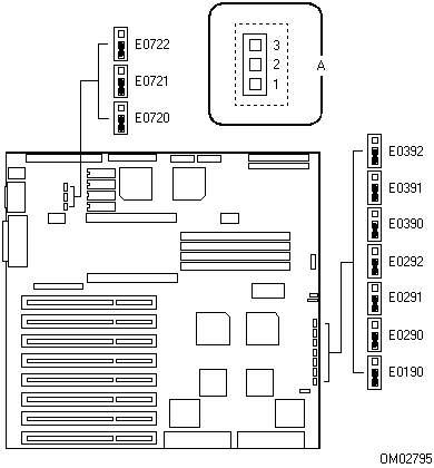
Flash Memory Jumper E0190
The flash memory jumper enables the BIOS flash memory special recovery mode. The system BIOS can be corrupted, for example: when the update procedure is aborted due to a power outage. The flash memory contains a protected area that cannot be corrupted. Code in this area is used to boot the computer from drive A when the BIOS has been corrupted. After booting, the flash update utility is used to automatically recover the system BIOS from the BIOS recovery files on the diskette.
CAUTION: To reprogram the BIOS, you need to ensure that the flash reprogramming power jumper E0721. is on pins 1 and 2, the default position. Do not change the NVRAM jumper E0292 at the same time.
Note: The flash reprogramming power jumper E0721 must be in the +12 V position, pins 1 and 2, during flash programming. Moving the jumper to pins 2 and 3 disables the ability to write to the flash memory. However, the jumper should be left in the +12 V position, pins 1 and 2.
If you have mapped the BIOS of an add-in board to any part of the E0000H address range, you must either map it to another area or physically remove the board from the system before a recovery procedure can be completed. You do not have to remove add-in boards for normal BIOS updates.
Recover the BIOS by doing the following:
1. Observe the precautions listed under Before You Begin Moving Jumpers.
2. Remove the system covers as described in your product guide.
3. Ensure that the flash reprogramming power jumper, E0721, is on pins 1 and 2 (default). This puts +12 V on the program pin of the flash BIOS components.
4. Move the flash memory boot jumper, E0190., from pins 1 and 2 (default) to pins 2 and 3.
5. Replace the system covers as described in your product guide.
6. Insert the flash memory update diskette in drive A.
7. Connect the power cord to the system and turn it on. After the system boots successfully, the speaker emits a single beep and the recovery process starts, which takes about three minutes.
While in the recovery mode, there is no screen display on the monitor and the keyboard is disabled as the system automatically recovers the BIOS. Because there is no screen display, the recovery status is identified through these beep codes.
Beep Code | Message |
2 | Successful completion, no errors. |
4 | The system could not boot from the diskette. The diskette may not be bootable. |
Continuous series of low beeps | The wrong BIOS recovery files are being used and/or the flash memory jumper E0721 is not set properly. |
8. When the recovery process completes, the system speaker emits two beeps indicating a successful completion of the process.
9. Turn the system off and remove the covers.
10. Move the flash memory boot jumper, E0190, from pins 2 and 3 to pins 1 and 2 (default).
11. Replace the system covers.
12. Remove the flash memory update diskette from drive A.
13. After running the special recovery mode, run the ECU to specify a new password.
VGA Jumper E0290
The VGA jumper controls the onboard video controller. In most cases the system detects an installed add-in board and disables the onboard video controller. If you suspect that the add-in board is not being detected correctly, disable the controller by doing the following:
1. Observe the precautions listed under Before You Begin Moving Jumpers.
2. Remove the system covers as described in your product guide.
3. Move the video jumper E0290A9IE9. from pins 1 and 2 to pins 2 and 3.
4. Replace the system covers as described in your product guide.
5. After disabling the onboard video controller, run the ECU to specify the new setting.
Floppy Protection Jumper E0291
The floppy protection jumper is used as a security device that controls writing to diskettes in the system diskette drives. For example, it can be used to prevent users from copying information from the system hard disk drives to a diskette. To write protect a disktte drive with this jumper, do the following procedure:
1. Observe the precautions listed under Before You Begin Moving Jumpers.
2. Remove the system covers as described in your product guide.
3. Move the floppy protection jumper, E0291A9IE9., from pins 1 and 2 to pins 2 and 3.
4. Replace the system covers as described in your product guide.
NVRAM Jumper E0292
To reset the system's NVRAM and real-time clock (RTC) chip to factory default values, do the procedure listed below.
Note: The flash reprogramming power jumper E0721 must be in the +12 V position, pins 1 and 2 (default)., during NVRAM programming. Moving the jumper to pins 2 and 3 disables the ability to write to NVRAM. However, the jumper should be left in the +12 V position, pins 1 and 2.
1. Observe the precautions listed under Before You Begin Moving Jumpers.
2. Remove the system covers as described in your product guide.
3. Move the NVRAM jumper E0292. from pins 1 and 2 to pins 2 and 3.
4. Ensure that the flash reprogramming power jumper, E0721, is on pins 1 and 2 (default). This puts +12 V on the program pin of the flash BIOS components.
5. Replace the system covers as described in your product guide.
6. Connect the power cord to the system, turn the system on, and wait for POST. to complete. This will automatically reprogram the NVRAM and RTC to their default settings.
7. Turn the system off and disconnect the power cord from the system.
8. Remove the system covers.
9. Move the NVRAM jumper E0292 from pins 2 and 3 back to pins 1 and 2.
10. Replace the system covers.
11. After resetting the NVRAM, run the ECU to configure your system if possible, if not, run the Setup utility.
Password Jumper E0390
To clear your system password, do the following procedure:
1. Observe the precautions listed under Before You Begin Moving Jumpers.
2. Remove the system covers as described in your product guide.
3. Move the password jumper E0390. from pins 1 and 2 to pins 2 and 3.
4. Replace the system covers as described in your product guide.
5. Connect the power cord to the system, turn the system on, and wait for POST. to complete. This automatically clears the password.
6. Turn off the system and disconnect the power cord.
7. Remove the system covers.
8. Move the password jumper E0390 back to pins 1 and 2.
9. Replace the system covers.
10. Run the ECU to specify a new password.
SIMM0 Jumper E0391
The SIMM0 jumper is set to STD (standard) mode, the default position pins 1 and 2, when bank 0 contains 1 MB, 2 MB, 4 MB, or 8 MB SIMMs. For 16 MB or 32 MB SIMMs, this jumper must be moved to pins 2 and 3.
Note: Bank 0 refers to SIMM sockets J0550 and J0551 on the system baseboard.
To increase the bank 0 size, do the following procedure:
1. Observe the precautions listed under Before You Begin Moving Jumpers.
2. Remove the system covers as described in your product guide.
3. Move the SIMM0 jumper E0391. from pins 1 and 2 to pins 2 and 3.
4. Replace the system covers as described in your product guide.
SIMM1 Jumper E0392
The SIMM1 jumper is set to STD (standard) mode, the default position pins 1 and 2, when bank 1 contains 1 MB, 2 MB, 4 MB, or 8 MB SIMMs. For 16 MB or 32 MB SIMMs, this jumper must be moved to pins 2 and 3.
Note: Bank 1 refers to SIMM sockets J0650 and J0651 on the system baseboard.
To increase the bank 1 size, do the following procedure:
1. Observe the precautions listed under Before You Begin Moving Jumpers.
2. Remove the system covers as described in your product guide.
3. Move the SIMM1 jumper E0392. from pins 1 and 2 to pins 2 and 3.
4. Replace the system covers as described in your product guide.
Video Memory Jumper E0720
The video memory jumper allows you to increase the onboard video buffer size from 512 KB to 1 MB.
Note: Only DRAMs from certain manufacturers have been tested for compatibility with the X-series deskside/LX system. Contact your sales representative or dealer for a list of approved manufacturers and their devices.
The following procedure tells how to increase the buffer size:
1. Observe the precautions listed under Before You Begin Moving Jumpers.
2. Remove the system covers as described in your product guide.
3. Install four, 256 K x 4, 60 ns DRAMs in the following system baseboard sockets: U0730, U0731, U0732, and U0830.
4. To increase the onboard video buffer size from 512 KB to 1 MB, move the video memory jumper E0720. from pins 1 and 2 to pins 2 and 3.
5. Replace the system covers as described in your product guide.
Flash Reprogramming Power Jumper E0721
When the flash reprogramming power jumper is on pins 2 and 3, the flash BIOS is protected and cannot be updated. This setting also protects the BIOS and EISA Configuration information and does not allow the user to change any system settings. The default position, pins 1 and 2, lets the user enter and modify selections with the ECU or Setup utility. To use or run these utilities, do the procedure listed below.
Note: When you install EISA add-in boards in your system, you must use the ECU to modify the flash.
CAUTION: Ensure that the flash reprogramming power jumper E0721. is on pins 1 and 2 (default). Do not change the NVRAM jumper E0292 at the same time.
1. Observe the precautions listed under Before You Begin Moving Jumpers.
2. Remove the system covers as described in your product guide.
3. Ensure that the flash reprogramming power jumper E0721 is on pins 1 and 2.
4. Replace the system covers as described in your product guide.
5. Connect the power cord to the system, turn the system on, and wait for POST. to complete.
6. Reboot the system with the ECU diskette or enter Setup to update the BIOS.
If you want to write-protect the flash memory, move the flash reprogramming power jumper E0721 to pins 2 and 3. To do this, repeat steps 2 and 4 above.
Video Address Jumper E0722
The video address jumper determines which I/O port the onboard Western Digital WD90C31 super VGA controller uses for its internal AT mode setup port. The starting address of the default port is 03C3H. To change the starting address to 46E8H, do the following procedure:
1. Observe the precautions listed under Before You Begin Moving Jumpers.
2. Remove the system covers as described in your product guide.
3. Move the video address jumper E0722. from pins 1 and 2 to pins 2 and 3 to change the starting address of the I/O registers to 46E8H.
4. Replace the system covers as described in your product guide.
Memory Map
Address Range | Amount | Function |
00000H to 07FFFH | 512 KB | Base system memory |
80000H to 9FFFFH | 128 KB | Base memory enabled in Setup |
0A0000H to 0BFFFFH | 128 KB | Video RAM |
0C0000H to 0C7FFFH | 32 KB | Off board video BIOS (can be shadowed) |
0C8000H to CFFFFH | 32 KB | Adapter BIOS extensions (can be shadowed) |
0D0000H to DFFFFH | 64 KB | Adapter BIOS extensions |
0E0000H to 0E7FFFH | 32 KB | Onboard WD90C31 video BIOS (can be shadowed) |
0E8000H to E9FFFH | 8 KB | EISA configuration data |
0EA000H to 0EBFFFH | 8 KB | OEM user memory area |
0EC000H to 0EFFFFH | 16 KB | Recovery BIOS |
0F0000H to FFFFFH | 64 KB | System BIOS |
100000 to FFFFFFF | 15 MB | Extended Memory |
0C8000H to 0DFFFFH | 96 KB | Reserved for ROM and RAM on addin boards |
0H to 800FFFFFH | 2 GB�+ 1�MB | Limit of the X-series architecture |
Related Topics:
Graphic View of System Memory Map
Graphic View of System Memory Map
A, extended memory; B, high memory; C, conventional memory; D, flash ROM area; E, video BIOS alias area; F, video memory; G, system BIOS; H, recovery BIOS (16�KB); I, user area (8 KB); J, EISA configuration (8 KB); K, video BIOS (32�KB).
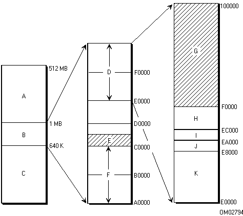
I/O Map
I/O Address | Device |
000 - 00F | Slave DMA controller 1 |
020 - 021 | Master Interrupt controller 1 |
026 | Configuration controller index registers |
027 | Configuration controller data registers |
040 - 043 | Interval timer 1 |
048 - 04B | Interval timer 2 |
060, 064 | Keyboard/mouse controller |
061 | NMI and diagnostic port |
070 | Real-time clock |
070 | Enable NMI |
071 | Real-time clock |
078 | BIOS loop timer |
080 | Power-on self test (POST) error codes |
081 - 08F | DMA page register |
092 | System control port |
0A0 - 0A1 | Slave interrupt controller 2 |
0C0 - 0DE | Master DMA controller 2 |
0F0 | Reset numeric coprocessor |
0F8 - 0FF | Numeric coprocessor |
1F0 - 1F8 | IDE hard drive controller |
278 - 27B | Parallel port 2 (LPT2); parallel port 3 (PS/2-compatible) |
2C0 - 2DF | Clock calendar |
2E8 - 2EF | Serial port 4 (COM4) |
2F8 - 2FF | Serial port 2 (COM2) |
378 - 37F | Parallel port 1 (LPT1); parallel port 2 (PS/2-compatible) |
3B0 - 3BB | WD90C31 onboard video registers |
3BC - 3BE | Parallel port 3 (LPT3); parallel port 1 (PS/2-compatible) |
3BF - 3DF | 16C552 registers |
3E8 - 3EF | Serial port 3 (COM3) |
3F0 - 3F5 | Onboard floppy controller |
3F6 | Onboard IDE hard drive controller |
3F7 | Onboard IDE read |
3F7 | Onboard Floppy controller read/write |
3F8 - 3FF | Serial port 1 (COM1) |
400 - 40B | Extended DMA controller 1 registers |
40C - 40F | Extended control/test registers |
461 - 464 | Extended NMI register |
464 - 465 | Extended bus master |
480 - 48F | Extended DMA page register |
4C2 - 4CE | Extended DMA 2 registers |
4D0 | Extended interrupt 1 |
4D1 | Extended interrupt 2 |
4D4 | Extended DMA 2 chaining |
4D4 | Extended DMA 2 write mode |
C02 - C04 | System baseboard configuration information |
C80 - C83 | System baseboard EISA ID register |
C84 | System baseboard enable |
C85-C87 | Reserved |
9xxx-9FFF | Onboard AIC-7770 SCSI controller |
Interrupts
IRQ | Device |
NMI | Parity error |
0 | Reserved, interval timer |
1 | Reserved, keyboard buffer full |
2 | Reserved, cascade interrupt from slave PIC |
3 | Onboard serial port 2 (COM2), if enabled |
4 | Onboard serial port 1 (COM1), if enabled |
5 | LPT2, if enabled |
6 | Onboard floppy controller, if enabled |
7 | LPT1, if enabled |
8 | Real-time clock (RTC) |
9 | User definable; it can be set for EISA add-in boards using the ECU |
10 | COM3; if enabled, it can be set for EISA add-in boards using the ECU |
11 | COM4; if enabled, it can be set for EISA add-in boards using the ECU |
12 | Onboard PS/2 mouse port, if enabled |
13 | Reserved, math coprocessor |
14 | IDE hard drive controller, if enabled |
15 | User definable; using the ECU, it can be set for the following: � EISA add-in boards � IDE hard drive controller � onboard video, programmable to 9, 10, 11, or 15 � onboard SCSI, programmable to 9, 10, 11, or 15 (ECU limits SCSI to three choices) |
Direct Memory Access (DMA) Channels
Channel | Device |
0 | (add-in board) |
1 | (add-in board) |
2 | Floppy disk drive |
3 | IDE hard disk drive |
4 | Reserved |
5 | (add-in board) |
6 | (add-in board) |
7 | (add-in board) |
System Baseboard SIMMs
The system baseboard contains four SIMM sockets: J0550 and J0551 (bank 0) and J0650 and J0651 (bank 1). Each socket can hold a single-sided or a double-sided, 80 ns, 36-bit fast-page SIMM module with a capacity of 1, 2, 4, or 8�MB. Each socket can also hold a singlesided or a doublesided, 70 ns, 36-bit fast-page SIMM module with a capacity of 16 or 32�MB. The baseboard will support up to 128 MB with four 32 MB SIMMs. Different-size SIMMs can be mixed in the system; however, they must be installed in like-sized pairs. Each pair can be of different size. You can install SIMMs in two or all four of the SIMM sockets (one or three installed SIMMs are not supported).
For information about the system memory map, see "System Baseboard"
For information about setting the SIMM memory bank jumpers, see "SIMM0 Jumper E0391" and "SIMM1 Jumper E0392"
When you install SIMMs in the sockets on the baseboard, you must start with socket J0550. When you remove SIMMs from the sockets, you must start with the first SIMM-filled socket closest to the CPU module connector J0770.
CAUTION: Mixing dissimilar metals may cause failures.
� SIMMs with tin-lead alloy plated edge connectors must be installed only in tin-lead alloy plated sockets.
� SIMMs with gold-lead alloy plated edge connectors must be installed only in gold-lead alloy plated sockets.
Note: Only SIMMs from JEDEC-compatible manufacturers have been tested for compatibility with the X-series deskside/LX system. Contact your sales representative or dealer for a list of approved devices.
Related Topics:
Baseboard SIMM Jumpers
Installing System Baseboard SIMMs
Baseboard SIMM Jumpers
The table below lists the jumpers and their factory default settings for each memory bank on the baseboard. If you install a pair of 16 MB or 32 MB SIMMs, you must move the memory bank jumper. from pins 1 and 2 to pins 2 and 3. In the figure, A shows the locations of the baseboard SIMM sockets.
Bank | Jumper | Position | SIMM Size | SIMM Speed |
0 (J0550 and J0551) | E0391 | 1 to 2* | 1, 2, 4, and 8 MB | 70 ns or 80 ns |
1 (J0650 and J0651) | E0392 | 1 to 2* | 1, 2, 4, and 8 MB | 70 ns or 80 ns |
* Factory default setting.
Installing System Baseboard SIMMs
When properly installed, the SIMM module is oriented at an angle of 90� relative to the system baseboard; see F in the figure.
CAUTION: Use extreme care when installing a SIMM module. Applying too much pressure can break the retaining clips or damage the socket slot.
Note: SIMM modules are keyed and can be inserted in only one way.
1. Observe the precautions listed under "Before You Begin Moving Jumpers."
2. Remove the system covers, CPU module, and memory module (if installed) as described in your product guide.
3. Holding the SIMM module only by the edges, remove it from its antistatic package.
4. With the notched edge of the SIMM (E in the figure) facing towards the left edge of the system baseboard, position the SIMM at about a 45� angle relative to the socket on the baseboard (1 in the figure). The small notch in the middle of the bottom edge of the SIMM mates with the raised bump in the SIMM socket.
Beginning with socket J0550, insert the bottom edge of the SIMM into the socket and press in firmly on the SIMM until it seats correctly (1 in the figure).
5. When the SIMM seats correctly, hold it at each end and gently push the top edge towards the retaining clips (C in the figure) of the socket connector until the SIMM snaps into place (2 in the figure). The small horizontal posts by the retaining clips will pass through the holes in the ends of the SIMMs (F in the figure).
If the SIMM does not install correctly, gently push the retaining clips in opposite directions just enough so that you can pull away the top edge of the SIMM and try again.
6. Repeat the above steps to install the remaining SIMMs in the sockets. Fill the sockets in this order: J0550, J0551, J0650, and J0651.
7. Replace the CPU module, memory module, and system covers as described in your product guide.
8. Run the ECU to properly attribute the additional memory. Failure to do so may degrade the performance of your system.
Note: Running Setup will not attribute the memory.
Installing the SIMMs
A, SIMM sockets; B,�SIMM module; C, retaining clip; D, SIMM socket; E, notched edge of SIMM; F, properly installed SIMM module.
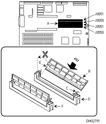
Related Topics:
Removing System Baseboard SIMMs
Removing System Baseboard SIMMs
CAUTION: Use extreme care when removing a SIMM. Too much pressure can break the retaining clips or damage the socket slot. Apply only enough pressure on the retaining clips to release the SIMM.
1. Observe the precautions listed under "Before You Begin Moving Jumpers."
2. Remove the system covers, CPU module, and memory module (if installed) as described in your product guide.
3. Remove the SIMM modules one at a time, starting with socket J0651, J0650, J0551, and J0550 (see A in the figure).
4. Gently push the retaining clips (1 in the figure) in opposite directions just enough so that you can tilt the top edge of the SIMM away from the clips (2 in the figure).
5. Carefully lift the SIMM away from the socket (3 in the figure) and store it in an antistatic package.
6. Repeat the above steps to remove the remaining SIMMs.
7. Replace the CPU module, memory module, and system covers as described in your product guide.
8. Run the ECU to properly attribute the remaining memory. Failure to do so may degrade the performance of your system.
Note: Running Setup will not attribute the memory.
Removing the SIMMs
A, SIMM sockets; B,�SIMM module; C, retaining clip; D, SIMM socket; E, properly installed SIMM module.
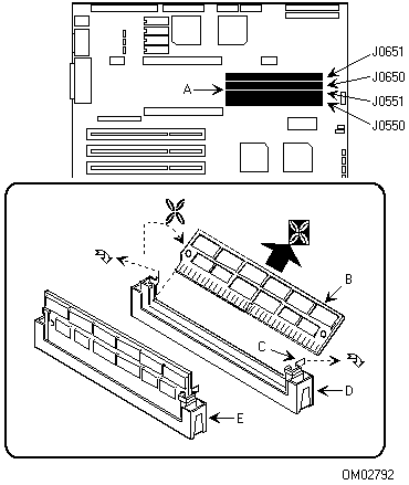
Video Memory DRAMs
The system baseboard comes with 512 KB of onboard video memory that allows pixel resolutions of 640 x 480 and 800 x 600 in 256 colors, and 1024�x�768 in 16 colors.
The video memory buffer size can be increased from 512 KB to 1 MB by installing four, 256 K x 4, 60 ns fast-page DRAMs in the following system baseboard sockets: U0730, U0731, U0732, and U0830. Adding these DRAMs allows 132 column text modes and pixel resolutions of 640 x 480, 800�x�600, and 1024 x 768 in 256 colors. Depending on the environment, the controller displays up to 32,000 colors in some video resolutions.
Note: Only DRAMs from certain manufacturers have been tested for compatibility with the X-series deskside/LX system. Contact your dealer or sales representative for a list of approved manufacturers and their devices.
For information about setting the video memory buffer size jumper, see "Video Memory Jumper E0720."
Related Topics:
Installing Video Memory DRAMs
Installing Video Memory DRAMs
1. Observe the precautions listed under "Before You Begin Moving Jumpers."
2. Remove the system covers as described in your product guide.
3. Remove a 256 K x 4, 60 ns DRAM from its protective package and align the notched end (C) of the DRAM (D) with the notched end of socket U0730 (E) on the baseboard.
4. Press the DRAM down firmly until it is fully seated in the socket (E). Be careful not to bend the pins.
5. Repeat steps 3 and 4 above successively to install DRAMs in sockets U0731, U0732, and U0830.
6. To increase the onboard video memory buffer size from 512 KB to 1 MB, move the video memory jumper E0720 from pins 1 and 2 to pins 2 and 3 (A).
7. Replace the system covers as described in your product guide.
DRAM Sockets
A, E0720 jumper pins (1 to 2, 512 KB) (2 to 3, 1 MB); B, DRAM and socket; C, key notch; D, DRAM chip; E, socket.

Related Topics:
Removing Video Memory DRAMs
Removing Video Memory DRAMs
1. Observe the precautions listed under "Before You Begin Moving Jumpers."
2. Remove the system covers as described in your product guide.
3. Find DRAM sockets U0730, U0731, U0732, and U0830 on the system baseboard.
4. To remove a DRAM from its socket, use a chip extraction tool. Gently pry up each end of the chip and pull it straight up out of the socket.
5. Place the DRAM on an antistatic surface.
6. Repeat the steps 4 and 5 successively to remove the remaining DRAMs.
7. To set the onboard video memory buffer size to 512 KB, the default setting, move the video memory jumper E0720 from pins 2 and 3 to pins 1 and 2 (A).
8. Replace the system covers as described in your product guide.
Parts List
Should you need to replace a part in your X-series deskside/LX system, you may find the parts list helpful. The illustrations for parts 1-7 and 8-13 show the parts by item number. For information about prices and delivery, contact your sales representative or dealer.
Item No. | Part No. | Description |
1 | 611945 | PBA (printed board assembly), system front panel board |
2 | 202123-001 | 230 watt power supply |
3 | 612413 | +12 volt fan (axial, variable speed) |
4 | 515524 | Module retaining bracket for CPU and memory modules |
5 | 616738-003* | Snap-in, black plastic, peripheral slide rail A, 616738-001 (no screws) |
6 | 616783-003* | Snap-in, black plastic, peripheral slide rail B, 616738-002 (no screws) |
7 | 611494-001 | Lock assembly with key |
8 | 507033-001 | Plastic filler panel for inner panel and door assembly |
9 | 516398 | Grounding clip for the peripheral snap-in slide rail |
10 | 610547 | Activity LED cable for SCSI hard disk drives (baseboard to host adapter board) |
11 | 613328-001 | Plastic front door bezel kit |
12 | 612060-001 | Chassis assembly (includes cover and bezels) |
13 | 611494-004 | Master key and lock assembly |
* Part number 616738-003 consists of five type A slide rails, 616738-001, and five type B slide rails, 616738-002.
Spare Parts (1-7) Illustration
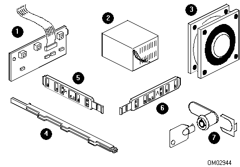
1 | 611945 | PBA (printed board assembly), system front panel board |
2 | 202123-001 | 230 watt power supply |
3 | 612413 | +12 volt fan (axial, variable speed) |
4 | 515524 | Module retaining bracket for CPU and memory modules |
5 | 616738-003* | Snap-in, black plastic, peripheral slide rail A, 616738-001 (no screws) |
6 | 616783-003* | Snap-in, black plastic, peripheral slide rail B, 616738-002 (no screws) |
7 | 611494-001 | Lock assembly with key |
* Part number 616738-003 consists of five type A slide rails, 616738-001, and five type B slide rails, 616738-002.
Spare Parts (8-13) Illustration
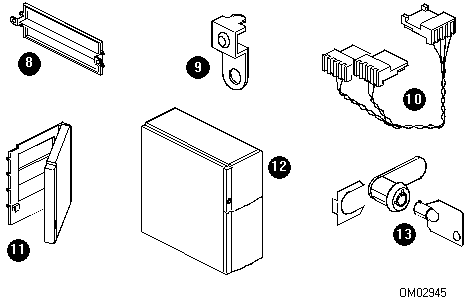
8 | 507033-001 | Plastic filler panel for inner panel and door assembly |
9 | 516398 | Grounding clip for the peripheral snap-in slide rail |
10 | 610547 | Activity LED cable for SCSI hard disk drives (baseboard to host adapter board) |
11 | 613328-001 | Plastic front door bezel kit |
12 | 612060-001 | Chassis assembly (includes cover and bezels) |
13 | 611494-004 | Master key and lock assembly |